
Aboutcs
About Compound Semiconductors
![CirclesOfProductivity]() Bring on the compound semiconductors
Bring on the compound semiconductors
 Bring on the compound semiconductors
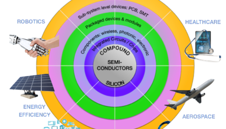
Impressive as the impact of silicon has been on our lives, it has a very basic and limited set of properties that restricts its application in many new and emerging technology areas that demand ultra-high performance levels along with sensing and other capabilities.
By atomically engineering crystal structures that combine elements either side of those in group IV of the periodic table (eg groups III and V), a set of new semiconductor materials has emerged whose enhanced properties offer significant performance improvements over those of silicon alone.
These compound semiconductors enable high speed processing in excess of 100 times that of silicon, as well as an array of other properties including the ability to emit and sense light, all the way from the infrared, through the visible and into the ultra-violet part of the spectrum.
Compound semiconductors have already complimented silicon in areas such as wireless communications, where chips made from material combinations such as gallium and arsenic (gallium arsenide, or GaAs) are found in virtually every smartphone where they enable high speed, high efficiency wireless communications in cellular and WiFi networks.
Other properties offered by compound semiconductor materials include the ability to emit and sense light in the form of general lighting (LEDs) and communications (lasers and receivers for fibre-optics).
The photonic and power efficiency properties offered by compound semiconductors that could not be achieved with silicon alone, will enable technologies essential in areas such as safety and security systems, healthcare technologies, aerospace and automotive applications including electrically powered and autonomous vehicles.
It is our ability to harness the advanced properties of the full range of semiconducting materials that will drive the digital revolution for generations to come.
Welcome to the world of advanced, compound semiconductors.
Epitaxy
Epitaxy is the materials technology that defines the performance and key characteristics of compound semiconductor enabled technologies.
The epitaxial growth process is a nanotechnology whereby complex atomic structures are produced under strictly controlled conditions. The end product is a pure, crystaline semiconductor wafer (substrate) upon which complex structures comprising many individual atomic layers are grown.
These epitaxial layers uniquely define the wireless, photonic and electronic performance of our epiwafers which are then processed by our customers to produce the “chips” that are found in virtually all of today’s technology devices and gadgets.
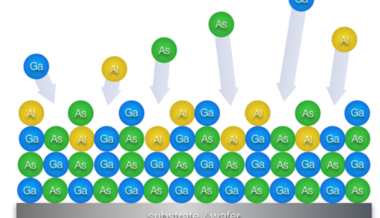
Epitaxy is the first key stage in the process of manufacturing the critical components in a wide range of devices from mobile handsets to solar cells and LEDs, and it requires high specification cleanrooms, sophisticated production tools and high levels of intellectual property.
