
Setting the reverse diode to strike may cause the Cloud Node or door controller to reboot. A diode damaged or blown (dead) can act as if there is no diode, installed backwards, or show incorrect data in the log such as card scan when the strike returns to the default state.
Which way does the band on a diode go?
Does it matter which way the diode goes? The positive side is called the anode, and the negative side is called the cathode. A diode circuit symbol, with the anode and cathode marked. The current through the diode can only flow from the anode to the cathode, which will explain why it is important for the diode to be connected in the right direction.
Is the band on a diode positive or negative?
Each diode has a colored dot or band printed on the cathode (negative) end of the component. A black plastic diode will have a white band painted on the cathode end and a glass diode will have a white or black band.
Is the line on a diode positive or negative?
Diode Polarity & Symbols One side is the positive terminal, called the anode. The other terminal is the negative end, called the cathode. Back to our electricity flow, now we can only move the diode from the anode to the cathode, never the other way around.
What does the band on a diode represent?
The band on the diode indicates the cathode or negative end of the device.
Which end of diode is positive?
The positive end of the diode is called the anode, and the negative end is called the cathode. Current can flow from the end of the anode to the cathode, but not in the other direction.
Which terminal of PN diode is positive?
In a forward biased p-n junction diode (p-type connected to the positive terminal and n-type connected to the negative terminal), the anode terminal is the positive terminal while the cathode terminal is the negative terminal. The anode terminal is a positively charged electrode or conductor, which supplies holes to the p-n junction.
Which diode leg is positive?
Like all other diodes current will only flow through the LED in one direction. In other words, LED has a positive and negative leg. The positive leg (called the anode) is easy to identify because it is the longer leg and the positive wire of the power supply should be connected to this leg.
How current flows through a diode?
When we connect a voltage source to a diode so that the positive side of the voltage source is connected to the anode and the negative side is connected to the cathode, the diode acts as a conductor, so that the current flows. When we connect a voltage to the diode in this direction, we call it forward bias.
How does a diode work? A diode where the junction emits light when current flows through the PN junction. When electricity flows through the semiconductor, the holes and electrons in the P-type semiconductor combine, and the energy is emitted as light. It is sometimes used as a power lamp and rectifier.
What does a diode do to current?
A diode is a semiconductor device that basically acts as a one-way switch for current. This allows current to easily flow in one direction, but severely restricts current from flowing in the opposite direction.
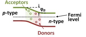
What is the difference between p-type and n-type semiconductor?
In an N-type semiconductor, electrons are the majority carriers and holes are the minority carriers. In P-type semiconductors, holes are the majority carriers and electrons are the minority carriers. In this substance, the majority of operators move from high to low potential.
What is the difference between n-type and p-type semiconductors How is each material formed? A p-type semiconductor is created when group III elements are doped into a fully semiconductor material. In contrast, n-type semiconductors are created when group V elements are doped into intrinsic semiconductors.
Which is better p-type or n-type semiconductor?
n-type tends to be a better choice due to reduced LID (Light Induced Degradation) & increased durability and performance compared to p-type.
Which has more holes p-type or n-type?
Impurities added in p-type semiconductor provide additional holes known as Acceptor atoms, while in n-type semiconductor impurities provide additional electrons and are called Donor atoms.
Why does n-type semiconductor has more conductivity than p-type?
Why is the conductivity of an n-type semiconductor greater than that of a p-type semiconductor even though both have the same doping level? Solution : The conductivity of n-type semiconductors is greater because the mobility of electrons is greater than that of holes.
What are the major four differences between n-type and p-type semiconductors?
| N-type semiconductor | P-type semiconductor |
|---|---|
| It has greater concentration of electrons and less concentration of holes. | It has a greater concentration of holes and less concentration of electrons. |
| Pentavalent impurities are added. | Trivalent impurities are added. |
What is the basic difference between P-type and n-type?
However, the key difference between the two is that P-type semiconductors are obtained by adding trivalent impurities like aluminum in pure semiconductors, while N-type semiconductors are obtained by adding pentavalent impurities like phosphorous in pure semiconductors.
What is the main difference between n-type and P-type semiconductors?
The basic difference between P-type and N-type semiconductors is that in n-type semiconductors, there is an excess of negative charge carriers. In a p-type semiconductor, there is an excess of positive charge carriers (holes, which can be considered as the absence of an electron).
What is hole effect?
The Hall effect is when a magnetic field is applied at right angles to the flow of current in a thin film where an electric field is generated, which is mutually perpendicular to the current and the magnetic field and which is directly proportional to the product of the current. density and magnetic induction.
What is the Hall effect in solid state physics? Hall effect, the development of a transverse electric field in a solid material when it carries an electric current and is placed in a magnetic field that is perpendicular to the current. This phenomenon was discovered in 1879 by the US physicist Edwin Herbert Hall.
What causes Hall effect?
The Hall effect is caused by the nature of the current in a conductor. Current consists of the movement of many small charge carriers, typically electrons, holes, ions (see Electromigration) or all three. When there is a magnetic field, this charge experiences a force, called the Lorentz force.
What triggers a Hall effect device?
Hall effect sensors are activated by magnetic fields and in many applications the device can be operated by a single permanent magnet mounted on a shaft or moving device. There are different types of magnet movements, such as âHead-onâ, âSidewaysâ, âPush-pullâ or âPush-pushâ etc.
What is Hall effect and what causes it?
Hall effect is a process in which a transverse electric field is developed in a solid material when a material carrying an electric current is placed in a magnetic field perpendicular to the current. The Hall effect was discovered by Edwin Herbert Hall in 1879.
What is classical Hall effect?
The classical Hall effect (discovered in 1879 by E. H. Hall) is also related to the motion of charge carriers in a magnetic field. It led to some of the earliest experiments that established the sign of charge carriers in conductors.
What is the formula of Hall effect?
The transverse voltage (Hall effect) measured in the Hall probe comes from the magnetic force on the moving charge carrier. The magnetic force is Fm = evdB where vd is the charge drift velocity.
What is the value of Hall effect?
The average value of the Hall coefficient was measured to be 0.0113±0.0002m3Câ1 and the sign of the positive Hall coefficient corresponds to the type of hole carrier and the sample is a p-type germanium crystal.
What is the formula of Hall voltage?
When calculating the Hall voltage, we need to know the current through the material, the magnetic field, its length, the number of charge carriers, and the area. Since all these are given, the Hall voltage is calculated as: v=IBlneA=(100A)(1.5T)(1.0×10â2m)(5.9×1028/m3)(1.6×10â19C)(2.0 ×10â5m2)=7.9×10â6V.

Comments are closed.