
Why n-type is better than p-type semiconductor?
Since n-type semiconductor has electrons as majority carriers and holes as minority carriers, while p-type semiconductor has holes as majority carriers and electrons as minority carriers, therefore the mobility of the n type is more than that of p type.
Which is better n-type or p-type? For one, since n-type cells use phosphorus instead of boron, they are immune to boron-oxygen defects, which cause reduced efficiency and purity in p-type structures. N-type cells are in turn more efficient and are not affected by light-induced degradation (LID).
Why do we use n-type semiconductor?
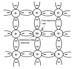
The fifth electron of the dopant is freed. Therefore, the impurity atom donates a free electron for conduction in the lattice and is called âDonarâ. Since the number of free electrons increases with the addition of an impurity, the negative charge carriers increase. Therefore, it is called an n-type semiconductor.
Why is n-type better?
Due to a lower degradation rate and improved technology N-Type panels last longer than P-Type, with warranty increases offered by a large number of N-Type panel manufacturers. Take Jinko for example , who’s 370W P-Type offers 12 years of warranty, compared to 20 years for the N-Type, an increase of more than 60%.
Which is better semiconductor n-type or p-type?
In n-type semiconductors, electrons are majority carriers, and holes are minority carriers. The electron density is much greater than the hole density in an n-type semiconductor denoted as ne >> nh whereas, in a p-type semiconductor the hole density is much greater than the of electrons nh >> ne.
Which type of semiconductor is best?
Silicon is the most widely used type of semiconductor material. Its main advantage is that it is easy to fabricate and provides good overall electrical and mechanical properties.
Which type of semiconductor is mostly used?
Since the early 1960s silicon has become by far the most widely used semiconductor, practically replacing germanium as a material for device fabrication.
Which is the best semiconductor of electricity?
Silicon is the best known of these as they form the basis of a large number of electrical circuits.
How does n-type semiconductor differ from p-type semiconductor?
In N-type semiconductors, electrons are majority carriers and holes are minority carriers. In P-type semiconductors, holes are majority carriers and electrons are minority carriers. In these substances, the majority carriers move from high to low potential. The majority carrier moves from lower to higher potential.
What is the difference between an n-type and a p-type semiconductor How is each material formed?
A p-type semiconductor is created when group III elements are doped for a complete semiconductor material. Conversely, an n-type semiconductor is created when group V elements are doped to an intrinsic semiconductor.
How is n-type and p-type semiconductors differ?
The basic difference between P-type and N-type semiconductors is that In an n-type semiconductor, there is an excess of negatively charged carriers. In a p-type semiconductor, there is an excess of positively charged carriers (holes, which can be seen as the lack of an electron).
What is the difference between acceptor and donor?
Donor / Acceptor Defined An acceptor is a low energy orbital with one or more vacancies: A donor is an atom or group of atoms whose highest filled atomic orbital or molecular orbital is higher in energy than that of a of reference.
Which is a donor or an acceptor semiconductor? In semiconductor physics, an electron donor is a dopant atom (impurity) that, when added to a semiconductor, can form an n-type semiconductor. An electron acceptor is a dopant atom (impurity) that, when added to a semiconductor, can form a p-type semiconductor.
What is difference between donor and acceptor impurity?
The donor impurity atom is having a total of 5 electrons in its valence shell. While the acceptor impurity is having 3 electrons in its valence shell. Due to the presence of extra electrons group V elements of the periodic table are considered a donor impurity.
What do you mean by donor impurity and acceptor impurity give example also?
Antimony, phosphorus and arsenic are group 15 elements, having 5 valence electrons. Therefore these are donor impurities. Whereas Indium is a group 13 element, having 3 valence electrons. Therefore Indium is an impurity that accepts.
What are donor and acceptor impurities Class 11?
1. Any pentavalent dopant atom that donates one electron for conduction is called a donor impurity. 2. Any trivalent atom that can accept an electron is called an acceptor impurity.
How can you tell if an element is a donor or acceptor?
The donor impurity atom consists of a total of 5 electrons in its valence shell. While the acceptor impurity atom consists of 3 electrons in its valence shell. The elements of Group V of the periodic table are considered a donor impurity due to the presence of extra electrons.
How do you identify a donor atom?
The donor atom is the atom within the ligand that is attached to the Lewis acid center. The coordination number is the number of donor atoms in the coordination complex. The denticity of a ligand is the number of bonds it forms with the Lewis acid center.
How do you identify an electron donor and acceptor?
Electron acceptors are ions or molecules that act as oxidizing agents in chemical reactions. Electron donors are ions or molecules that donate electrons and are reducing agents. In the combustion reaction of gaseous hydrogen and oxygen to produce water (H2O), two hydrogen atoms donate their electrons to an oxygen atom.
What is the difference between electron donor and acceptor?
Electron acceptors are ions or molecules that act as oxidizing agents in chemical reactions. Electron donors are ions or molecules that donate electrons and are reducing agents.
What is meant by electron acceptor?
An electron acceptor is a chemical entity that accepts electrons transferred to it from another compound. It is an oxidizing agent that, by virtue of its accepting electrons, is itself reduced in the process. Electron acceptors are sometimes mistakenly called electron receptors.
Which is an electron donor?
A nucleophile is an electron donor (has an electron pair available for bonding) that binds to an atom other than hydrogen. A base is an electron donor that bonds with hydrogen.
What is depletion layer in pn junction?
A depletion region or depletion layer is a region in a P-N junction diode where no mobile charge carriers are present. Reduction layer acts like a barrier that opposes the flow of electrons from the p-side and holes from the p-side.
How many depletion layers are there in the P-N junction? These two layers of positive and negative ions form the depletion region.
Why is there depletion layer in P-N junction?
Similarly, in semiconductors, the depletion region is the layer where the flow of charges slows down. This region acts as the barrier that opposes the flow of electrons from the n-side to the p-side of the semiconductor diode.
What happens to depletion region of pn junction?
Solution : If a p-n junction is reverse biased, the depletion region increases.
Why is depletion layer thin in forward bias?
In a P-N junction diode, the width of the depletion region decreases in forward bias. This is because the electrons are attracted to the positive terminal of the battery, so the negative ions disappear. Therefore, the forward bias narrows the depletion region, due to the carriers from the battery terminals.
What consists of depletion layer?
Note: The depletion layer consists of both electrons and protons but they are immobile in nature so the correct answer would be immobile ions. The donor and acceptor atom acquire a positive and negative charge due to which the PN junction is formed.
How many depletion layers are there in transistor?
A bipolar junction transistor (BJT) is a current-controlled device that performs its work using two PN junctions. There are also two areas of reduction. The bias condition applied to the connection determines the thickness of the depletion layer. Therefore the correct answer is the second.
Is there charge in a depletion layer?
The depletion region has only positive ions and negative forms due to the diffusion of carriers across the pn diode junction.
What is depletion layer and how it is formed?
The depletion region is caused by the diffusion of charges. Due to the concentration gradient holes diffuse from p-side to n-side across the junction while electrons diffuse from n-side to p-side. The holes and electrons that diffuse towards each other combine near the junction.
What is depletion layer and how it is formed in pn junction diode?
Electron movement towards the p-type side exposes positive ion cores in the n-type side while hole movement towards the n-type side exposes negative ion cores in -p-type side, resulting in an electron field in the junction and forming the depletion region.
Where are depletion layers formed?
In the semiconductor PN junction, electrons and holes recombine to produce a non-conducting depletion layer. If forward biased, the depletion layer is reduced, allowing current to flow according to an exponential relationship between current and forward voltage, as described in Section 9.5.
Is p-type the anode?
One terminal of the diode, known as the cathode, is connected to the n-type region. The other terminal, known as the anode, is connected to the p-type region. Electrons flow from the cathode to the anode.
P junction is an anode? The anode is a positive terminal in a forward biased p-n junction diode (the p-type is connected to the positive terminal and the n-type is connected to the negative). On this type of junction, the cathode terminal is negative.
Is p-type anode or cathode?
These holes act as positive charge carriers, and the region is called a p-type semiconductor material. One terminal of the diode, known as the cathode, is connected to the n-type region. The other terminal, known as the anode, is connected to the p-type region.
What is the P side of a diode?
The “p” (positive) side contains an excess of holes, while the “n” (negative) side contains an excess of electrons in the outer shells of the electrically neutral atoms there. This allows electrical current to flow through the junction in one direction only.
What is the p-type of the diode?
| Working principle | junction pan |
| Pin configuration | A: Anode, K: Cathode |
| Electronic symbol |
|---|
Is p-type semiconductor anode?
The current flows only in one direction, Along with the arrow, which corresponds to a forward bias. The cathode, bar, of the diode symbol, corresponds to an N-type semiconductor. The anode, arrow, corresponds to the P-type semiconductor.
What is p and N in PN junction diode?
In a semiconductor, the P-N junction is created by the doping method. The p-side or positive side of the semiconductor has an excess of holes, and the n-side or negative side has an excess of electrons.
What is p-type diode?
Electronic symbol. Diode pân is a type of semiconductor diode based on the pân junction. The diode conducts current in one direction only, and is made by combining a p-type semiconductor layer with an n-type semiconductor layer.
Is cathode p-type?
The schematic symbol of a PN junction diode is shown in the figure below. The vertical bar represents the cathode (N-type material) as it is the source of electrons. The arrow represents the anode (P-type material) as it is the destination of the electrons.
Is anode P-type in diode?
A diode is a rectifier, which allows current to flow in one direction but not in the opposite direction. When the anode (p-type side) of the diode is connected to the positive terminal of a battery, the diode is said to be in forward bias, allowing current to flow through it.
What type of electrode is a cathode?
The cathode is the negatively charged electrode. The cathode attracts cations or positive charge. The cathode is the source of electrons or donor of electrons.
Sources :

Comments are closed.