

In the underbelly of every digital device, we use today lies a marvel of modern science, a testament to the sophistication of human ingenuity – the silicon wafer. As we increasingly depend on semiconductor devices, understanding the fabrication of silicon wafers, the foundation of these devices, becomes paramount. This article demystifies the fascinating process of silicon wafer fabrication, illuminating the techniques that have revolutionized our digital age.
What is a Silicon Wafer?
At its core, a silicon wafer is a thin slice of highly pure, single-crystal silicon. It is the canvas upon which microcircuits are etched, thereby birthing the multitude of semiconductor devices that have altered our lifestyle in unimaginable ways.
Silicon Wafer Fabrication Techniques
- Silicon Ingot ProductionThe fabrication journey starts with the production of silicon ingots. Sand (silicon dioxide) is reduced in a high-temperature furnace, producing metallurgical-grade silicon. This is then chemically refined to produce highly pure polysilicon. Polysilicon is subsequently melted and formed into a single-crystal silicon ingot through a process known as Czochralski or the Float Zone process.
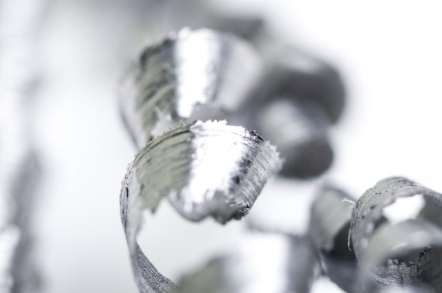
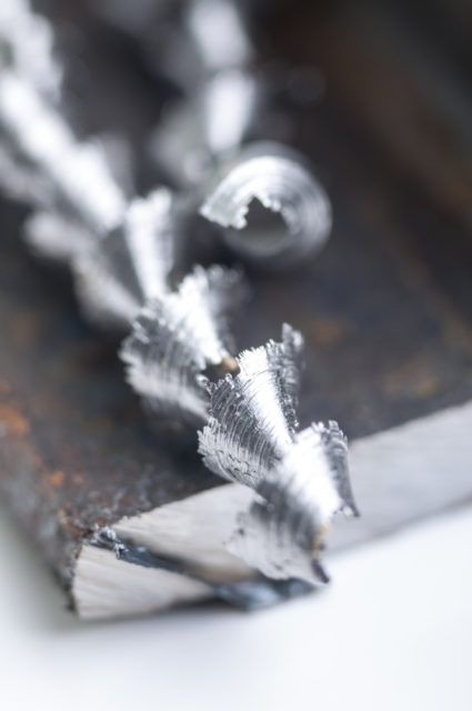
- Wafer SlicingThe cylindrical silicon ingot, sometimes weighing up to a few hundred kilograms, is then precisely sliced into thin wafers, usually with a thickness in the realm of 500-1000µm. This process employs an inner-diameter (ID) saw that uses a diamond-coated blade.
- Wafer Lapping, Polishing, and CleaningAfter slicing, the wafers are lapped to remove mechanical damage from the sawing process. They are then polished to achieve a mirror-like finish, which is essential for subsequent fabrication steps. Finally, a rigorous cleaning process is used to ensure the surface is free from contaminants.
- EpitaxyIn the epitaxy process, additional silicon is deposited onto the wafer in a highly controlled manner to form an epitaxial layer. This layer, which matches the crystal structure of the original wafer, is often used to introduce dopants that modify the electrical properties of the silicon.
- PhotolithographyThe artistry in silicon wafer fabrication truly shines in the photolithography process. Here, patterns defining microcircuits are transferred onto the wafer. This complex process, involving photoresist application, soft baking, mask alignment, exposure, development, and hard baking, helps in creating the essential architecture of our semiconductor devices.
- Etching and Ion ImplantationAfter photolithography, etching removes excess silicon, while ion implantation allows for precise control of dopant distribution. These processes enable the formation of p-n junctions, the basic units of semiconductor devices.
- Chemical Vapor Deposition (CVD) and Physical Vapor Deposition (PVD)These processes are used to deposit various materials onto the silicon wafer. CVD uses reactive gases, while PVD involves the condensation of vaporized forms of desired materials.
Conclusion
Silicon wafer fabrication is a remarkable technological achievement, a symphony of science and precision engineering that has sparked a revolution in information technology. With the demand for semiconductor devices showing no signs of abating, these fabrication techniques remain critical for propelling us further into the digital future.

Comments are closed.