
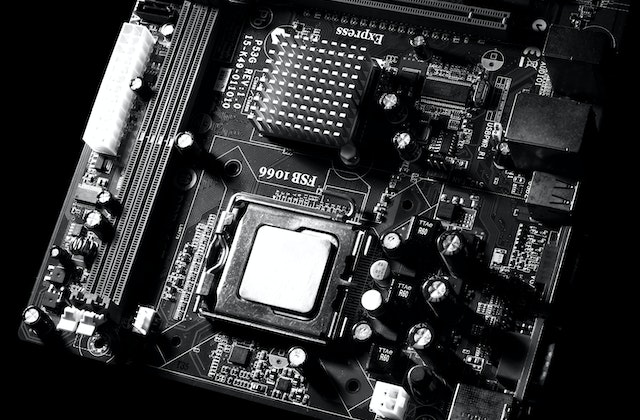
The semiconductor industry literally makes the world go round. Microchips are the heart of every computer, mobile phone, flat-screen TV and much more.
Emerging technologies like 5G and AI are spurring new demand for chips. Startups are developing tech-driven solutions to support these advancements.
Despite hiccups such as the COVID-19 pandemic, OCMs are pushing ahead with new fabrication facility construction to achieve domestic resiliency and global diversification.
More Moore
Half a century ago Gordon Moore, co-founder of Intel, predicted that the number of transistors that could be etched on a chip would double every year. Moore later revised his prediction to every two years, but either way it has remained an astonishingly accurate and self-fulfilling prophecy.
Moore’s Law has made possible everything from consumer electronics infused with artificial intelligence to cheaper, pint-size satellites for global atmospheric monitoring. It has fueled the economic growth and productivity that define our high-tech society.
But signs are mounting that More Moore is nearing an end. For example, the latest generation of chips produced by Intel is built with transistor features that are 10 nanometers wide, well beyond the minimum feature size that could be reliably produced using existing fab equipment.
More than Moore
For decades, the semiconductor industry has been able to shrink transistors and accommodate more of them on a chip. This has enabled significant advances in digital electronics, such as microprocessor performance, memory capacity and sensor technology, including those that detect cancerous cells, assist in autonomous driving and even take photos.
However, it’s now clear that the industry is entering a new era. As physics limits how small transistors can get, researchers are exploring other ways to boost computer power, beyond packing more silicon devices onto chips.
One promising approach is based on moving from traditional electronic transistors that transmit electrons to ones based on non-charge-based materials such as spin, molecular state, photons, phonons or nanostructures. This shift is expected to enable new capabilities such as enhanced security, quantum computing and 3D packaging.
Beyond CMOS
Technology is evolving faster than ever, creating new opportunities and posing fresh challenges for the semiconductor industry. Across segments, new technologies like AI and 5G infrastructure are creating sustained demand for semiconductors and spurring industry transformation.
The next generation of chips will require new materials and design techniques to move beyond silicon. IMEC is exploring several emerging devices and materials that can augment CMOS, including nano-photonics, tunneling FETs, and spintronics.
Similarly, emerging devices can be leveraged for efficient hardware accelerators to move computing paradigms forward. These devices can also help reduce security risk by simplifying circuit structures. These new functions are spurring More than Moore solutions, including miniature cameras, motion sensing, and biometric identification systems. They’re also driving demand for new noncomputational functions in consumer electronics.
2-D Materials
The semiconductor industry continues to evolve at a breakneck pace. New applications are driving technological development, spurring problem-solving and innovation.
2-D materials are a family of nanomaterials whose atomic layers are one or two atoms thick, including graphene. They are exceptionally strong, lightweight, flexible, and excellent conductors of heat and electricity.
Scientists at Brown University have discovered a way to directly manipulate the spin of electrons in these 2D materials. This breakthrough opens the door to developing computational and communicational devices that take advantage of the quantum mechanical properties of these materials. Other 2D materials include phosphorene, molybdenum disulfide, and transition metal dichalcogenides (TMDCs). These materials have a variety of band structures, making them promising candidates for optical devices and transistors. They also have the potential for biomedical applications.
Compound Semiconductors
Compound semiconductors, such as gallium arsenide (GaAs), silicon carbide (SiC), gallium nitride (GaN) and aluminium-gallium-indium-phosphide (AlGaInP), have emerged as important alternatives to silicon substrates in power electronics, radio-frequency applications, RF modules, and photonics including lasers, LEDs, and receivers for fiber optics. These innovative substrates have intrinsic properties that allow them to emit and sense electromagnetic radiation over a broad spectrum, from long-wavelength infrared to high-frequency visible and ultraviolet.
They have wider bandgap capabilities enabling better thermal performance, faster processing speeds, and lower power consumption than silicon chips. These benefits are crucial for addressing mega trends such as 5G, electric vehicles and hyper scale datacenters. They also offer the ability to handle the enormous amounts of data now being generated across industries. As a result, they are reshaping the future of technology.

Comments are closed.