
Intricately woven from two elements, namely gallium and arsenic, Gallium Arsenide (GaAs) is an outstanding class III-V semiconductor. Its structure draws inspiration from the Zinc Blende crystal formation. GaAs stands out with a number of unique traits that make it highly sought-after in myriad applications; for instance, its talent to emit infrared light when galvanized electrically grants it significant value for imaging endeavors.

Positioned favorably against materials such as silicon, GaAs revels in superior competence specifically in terms of detecting infrared radiation. This prowess can be predominantly accredited to indium’s involvement—an element plucked right off from the periodic table. When this constituent joins forces with Gallium Arsenide giving birth to Indium Gallium Arsenide (InGaAs), there is an amplification of attributes vital for identifying infrared light—these become indispensable particularly for spectrometry applications among numerous others.
The manufacturing process commences by developing epitaxial layers on a substrate utilizing techniques like molecular beam epitaxy or metal-organic chemical vapor deposition. The material thus shaped can subsequently be employed to fabricate devices such as diodes and lasers which boast high-speed electronics competencies complemented by efficient photovoltaics features. Moreover, InGaAs detectors have superiority over their pure gaas siblings both in sensitivity and noise performance making them more fitting candidates where precision holds paramount importance.
Role of Indium in Enhancing Gallium Arsenide’s Infrared Attributes
Submerged within the consortium of III-V semiconductors, Indium embodies an indispensable role in intensifying the infrared traits woven into Gallium Arsenide (GaAs). Its incorporation into GaAs induces a transformation in bandgap energy and augments absorption efficiency at extended wavelengths. This occurrence is triggered by Indium’s expanded atomic radius compared to gallium, causing a decrement in bandgap energy when it takes the seat of gallium atoms amidst the lattice formation. Consequently, detectors constructed from InGaAs outperform their silicon or germanium-based counterparts under near-infrared spectroscopy conditions.

The creation process initiates with employing an epitaxial growth technique on a GaAs foundation. Epitaxy encapsulates the concept of depositing one crystalline layer onto another; both being endowed with corresponding lattice formations. Infusing this semiconductor substance with indium not only reconditions its optical properties but also escalates its light emission efficacy – an attribute paramount for diode lasers incorporated in imaging applications. Moreover, InGaAs can be calibrated across diverse spectral ranges by regulating the indium to gallium ratio during fabrication.
Remarkably though more arduous to fabricate than conventional silicon or oxide semiconductors due to incongruent lattice constants and thermal expansion coefficients between layers; InGaAS offers numerous advantages over these alternatives particularly for pioneering sensor technologies. Gifted with high electron mobility and low noise characteristics make it ideal for deployment as photodetectors or image sensors demanding high sensitivity spanning broad spectral ranges – covering visible light through short-wave infrared (SWIR). Additionally, unlike germanium-based detectors which necessitate cooling systems due to susceptibility towards thermally generated dark currents at room temperature; uncooled operation becomes feasible with InGaAS detectors thereby simplifying system architecture while substantially curbing costs.
Insights into InGaAs: The Indium Gallium Arsenide Compound
Indium Gallium Arsenide, or InGaAs as it’s commonly referred to, is a composite semiconductor with an interesting array of optical attributes. This makes it the perfect candidate for tasks involving infrared detection and light emission. The refractive index that InGaAs boasts facilitates the absorption and emission of infrared light in an efficient manner – a quality that comes in handy when manufacturing photodiodes and laser diodes.
The epitaxial growth process contributes to this functionality by depositing slender films of InGaAs onto either a GaAs crystal or indium phosphide substrate. This forms an epitaxial layer elevating photon absorption capabilities within the device. Furthermore, this technique infuses regulated impurities into its structure, generating n-type GaAs layers which aid in enhancing infrared absorption.
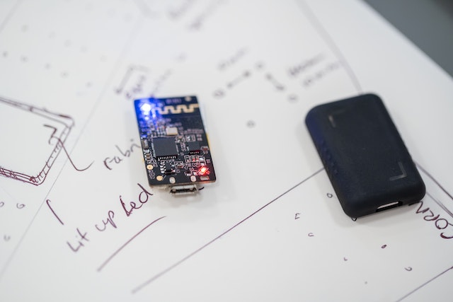
Post-deposition, there exists another vital step – etching. This process refines these features further by clearing away surplus material from the surface thereby providing precision for defining active regions where photons are absorbed or emitted within devices such as photodiodes and LEDs (light-emitting diodes). As depicted in Fig 1., thanks to meticulous design methods employed while constructing them, devices made from InGaAs are capable of detecting variations in infrared light at levels significantly more sensitive than those constructed with other materials like silicon.
Additionally, due to its inherent proclivity towards emitting light efficiently at longer wavelengths compared to standard LEDs; Indium Gallium Arsenide has gained substantial traction as a dependable source for near-infrared signals used extensively across telecommunication applications. Laser diodes created using this unique compound can function at high speeds whilst keeping power consumption low – crucial characteristics necessary for modern communication systems operations. Moreover, when fused together with avant-garde thin film technology techniques; these components deliver augmented performance abilities which far outstrip conventional options available on today’s market.
The Process of Fabricating GaAs for Infrared Applications
The intricate production of Gallium Arsenide (GaAs), particularly for infrared applications, calls for a meticulous and precise procedure. The metal-organic chemical vapor deposition (MOCVD) technique is commonly utilised in this regard. This process incorporates GaAs along with other elements such as gallium phosphide, augmenting the final product’s properties. Through MOCVD, better control over the GaAs surface can be achieved – a key factor when creating devices like diode lasers or cascade lasers where precision reigns supreme.
With their foundations set on GaAS, these laser types possess distinct features that make them ideal for certain applications. For example, they showcase high quantum efficiencies coupled with a direct band gap facilitating efficient conversion of electrical energy into laser light. These attributes are especially advantageous in shortwave infrared (SWIR) band detection and Fourier Transform Infrared spectroscopy where exactness in laser power makes all the difference. Furthermore, technologies based on GaAS such as CMOS sensors can be employed to construct more complex apparatuses including GaAS solar cells.
Enhancing gallium arsenide’s infrared capabilities even further involves integrating Indium Antimonide during fabrication stages. This compound expands absorption bands allowing detectors to function efficiently within far-infrared regions – an area typically challenging for traditional materials to effectively cover. Moreover, manipulating conditions during MOCVD growth phases allows optimization of different layers within photodetectors individually which leads to superior overall performance levels obtained through this holistic approach towards device creation.
Benefits of GaAs over Silicon in Infrared Detection
Immersed in a state of continuous evolution, the sphere of semiconductors has been experiencing an upsurge in the utilization of Gallium Arsenide (GaAs). This intriguing material, with its captivating properties, is becoming increasingly favored for crafting detectors that operate seamlessly within infrared territories. Far from being ordinary, this wide band gap semiconductor outperforms conventional materials like silicon by leaps and bounds – particularly when it comes to sensing and imaging applications.
It’s vital to keep in mind though, that indium – another character on this stage – despite enhancing GaAs’s infrared qualities cannot overstep its permitted boundaries. Overuse indeed threatens to disrupt harmony and balance.
What sets GaAs apart from other semiconductors? The answer lies hidden within its direct bandgap attribute which opens a gateway for superior performance in light-emitting applications pertaining to the infrared spectrum. It effortlessly overshadows those composed of silicon due to a considerably widened energy band gap which promises robust high-temperature performance coupled with elevated frequencies.
Further adding feathers into GaAs’s cap is its capacity to serve as a substrate upon which intricate circuits can be built. Researchers have time and again witnessed successful monolithic integration on these substrates – thereby further bolstering their faith in GaAs’s potential. Nonetheless, third-party substances not fitting within these constraints might introduce unforeseen limitations.
To establish credibility beyond doubts or disputes various methodologies are employed aimed at comparing these avant-garde semiconductors against traditional ones such as silicon. These investigative ventures invariably throw light on how gallium arsenide stands tall owing to unique physical attributes that make it compatible for specialized technologies needing enhanced power or frequency capabilities without necessitating any sacrifice regarding device size or cost-effectiveness.

Comments are closed.