
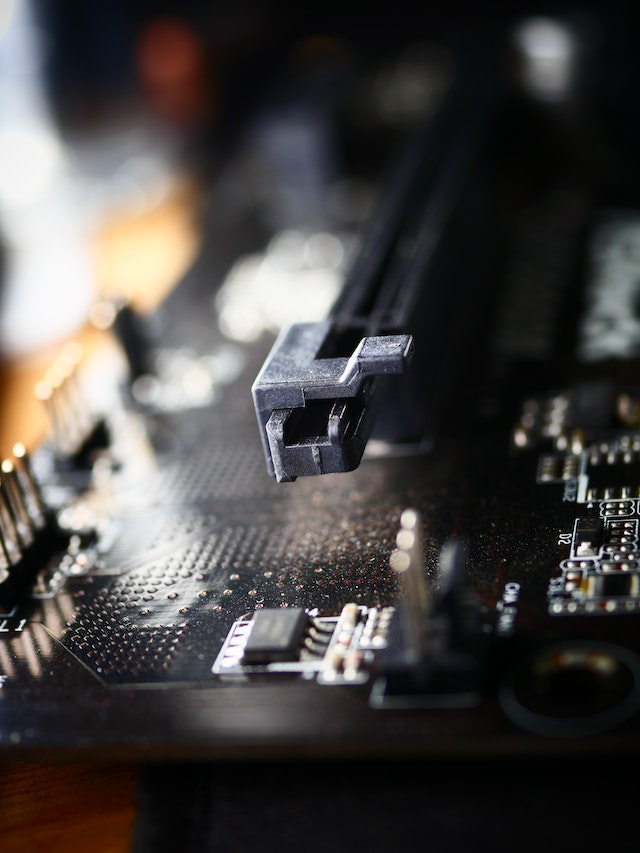
The binary semiconductor known as Indium Phosphide (InP), boasts a reputation resonating with high electron velocity and semi-insulating properties. Such features make it an ideal candidate for the crafting of integrated circuits (ICs). ICs birthed from InP demonstrate superior frequency handling prowess, outpacing counterparts crafted from alternate materials. This attribute empowers them to operate efficiently in environments pulsing with high-frequency, skyrocketing their value in the realm of modern electronics.

Diving deeper into the world of transistors – which serve as pillars bolstering electronic circuits by regulating electricity flow – one encounters InP’s unique attributes that drive unparalleled performance levels. Transistors built on InP gain enhanced efficiency, thermal stability fortitude, and signal processing speed acceleration. The application scope for this technology spills over traditional IC boundaries and has carved new pathways towards advancements in Heterojunction Bipolar Transistor Technology.
Heterojunction Bipolar Transistor technology taps into the distinct advantages gifted by diverse semiconducting materials. An exemplar is the Indium Phosphide Heterojunction Bipolar Transistor; integrating InP within its structure supercharges performance metrics while maintaining power efficiency at prime levels. This integration gifts these transistors with resilience against overheating or energy loss problems usually plaguing other types of transistors embedded within a circuit board. As we stand amidst continuous evolution in IC technology, anticipation builds around further enhancements set to maximize potential benefits sprouting from employing Indium Phosphide as a critical component within these systems.
Exploring the Use of Indium Phosphide in ICs
The semiconductor industry has been thrown into a state of intrigue by the rise of Indium Phosphide (InP). Its properties, unique and desirable, make it an apt choice for integrated circuits (ICs). The attraction towards InP is largely due to its capability to function at high frequencies – often soaring to gigahertz levels. This attribute makes it a covetable option for applications where speed and performance are paramount. Moreover, compared with their silicon counterparts, ICs crafted from InP display superior electron velocity and thermal conductivity.

Indium Phosphide’s reach permeates further into Heterojunction Bipolar Transistor (HBT) technology realms. When these two technologies are fused together- coined as Indium Phosphide Heterojunction Bipolar Transistors – they pave the way towards achieving loftier frequency operations in ICs. Their excellent high-frequency characteristics married with low noise figures have earned them recognition as formidable weapons within the compound semiconductor industry. According to IEEE reports, these transistors uphold outstanding performance even amidst harsh temperature conditions amplifying their applicability in robust circuit designs.
The amalgamation of InP with transistor development has spurred new paths for progressive IC technology. It empowers engineers not only to conceive more proficient circuits but also aids significantly in diminishing power consumption – an imperative aspect given today’s escalating demand for energy-efficient contrivances. Additionally, considering its compatibility with prevailing manufacturing procedures, embracing InP does not warrant drastic alterations on the production front rendering it a cost-effective solution too.
Unleashing the Power of Indium Phosphide ICs
Bursting onto the scene, Indium Phosphide ICs have swirled into prominence within the semiconductor industry, sending ripples through its core with their distinct attributes and multifaceted applications. Their resounding advantage lies in their blistering speed, a trait that transforms them into an ideal choice for power amplifiers and various devices craving rapid signal transmission. This lightning-fast competence is further bolstered by superior electron mobility gifted by Indium Phosphide.
Yet it would be remiss to reduce the role of Indium Phosphide to merely boosting speed; this material takes center stage in escalating device performance as well. Its innate traits like escalated breakdown voltage and density make it shine brightly as an exceptional substrate for heterojunction bipolar transistor (HBT) technology—a popular player in Radio Frequency (RF) applications. The InP HBT strides forth offering unparalleled linearity and efficiency—attributes that render it fitting for both wireless and optical communication systems.
The intrigue around Indium phosphide ICs doesn’t end here though—it extends deeper within analog circuits with their inherent low noise features. These elements pave way for purer signal processing which ultimately elevates system reliability several notches higher. With progressive leaps taken in HBT technology coupled with the sturdiness offered by indium phosphide substrates, there appears a vast landscape ripe for exploration—ushering us towards novel possibilities dotting the horizon of semiconductor innovation.
The Function of InP in Transistor Development
In the fascinating world of transistor development, Indium Phosphide (InP) stands as a cornerstone, particularly in reference to the realm of InP Heterojunction Bipolar Transistor (HBT) technology. The intriguing properties unique to InP establish it as an optimum compound semiconductor for high-speed integrated circuit applications – a wonder indeed.
The creation process is nothing short of artistry, involving the formation of monolithic structures capable of delivering staggering data rates and broad bandwidths – fundamental elements for advanced IC technology.
Enlightening discussions at forums like IEEE GaAs IC Symposium have brought forth wide-ranging debates on applying InP HBT technology. Esteemed experts such as Raghavan have emphasized its potentiality in revolutionizing circuit design. A noteworthy benefit lies in its capacity to fabricate circuits that operate at speeds surpassing those crafted with conventional CMOS technologies. This attribute renders InP-based devices especially valuable for telecommunications systems dependent on high data rate transmission.
Furthermore, progressions in indium phosphide heterojunction bipolar transistor fabrication processes have unveiled uncharted territories for integrating this compound semiconductor into existing IC technologies. Such integration not only enhances overall performance but remarkably boosts system efficiency by curtailing power consumption and heat generation – two critical challenges plaguing modern integrated circuits designs. Thusly, the role played by InP within transistor evolution continues to be instrumental in propelling advancement within the semiconductor industry’s landscape.
Intricacies of IC Circuit Design with Indium Phosphide
In the enigmatic sphere of electrical engineering, there’s been a seismic shift with the advent of Indium Phosphide (InP) in Integrated Circuit (IC) design. This unique semiconductor material and its kin boast superior traits that have radically transfigured high-speed circuit design – a fact emphatically underscored by Gopal Raghavan’s groundbreaking investigations into InP-based Heterojunction Bipolar Transistor (HBT) IC technology. The unparalleled features of InP, such as elevated breakdown voltage and swift transit time, render it a favored contender for device technologies where velocity is king.
Indium Phosphide claims an essential part in amplifying communication systems’ frequency range capabilities, thus enhancing their overall efficiency. Epitaxy techniques are harnessed to fabricate layers of InP which enable advanced electron devices to operate at higher frequencies than what was formerly achievable with alternative materials. One can witness this application vividly illustrated in frequency divider circuits wherein static frequency elevation is attained via capitalizing on the expedited transit time proffered by Indium phosphide and associated materials.
Optoelectronic ICs also seize advantage from exploiting Indium Phosphide due to its capacity to function at extreme velocities without undermining efficiency or dependability — vital attributes intrinsic to HBT ICs’ functionality. This positions them perfectly for utilization within intricate communication systems craving high-speed data transmission while preserving low power consumption levels. Thus, proclaiming indium phosphide’s contribution extends beyond mere device technologies wouldn’t be far-fetched; indeed, it constitutes an indispensable element of contemporary electronic infrastructure enabling seamless connectivity across diverse platforms.
Diving into the World of Heterojunction Bipolar Transistor Technology
In the realm of microelectronics, the advent of Heterojunction Bipolar Transistor (HBT) technology – more specifically indium phosphide heterojunction bipolar transistors – has ushered in a wave of transformative change. Notably, this state-of-the-art transistor architecture is celebrated for its ability to function at elevated frequencies and deliver performance levels that outshine other transistor technologies. The capacity for such high-speed operation can be attributed to decreased electron transit time, made possible by the distinctive material characteristics of indium phosphide.
The fabrication process entails molecular beam epitaxy – an approach utilized in creating strata of III-V compound semiconductors like Indium Phosphide (InP). ICs constructed on indium phosphide technology using InP HBT have seen widespread adoption within radio frequency environments and military domains due to their extraordinary cutoff frequencies and resilience even under severe conditions. These aspects render them the perfect selection when it comes to circuit design and process development where reliability, speed, and accuracy are crucial.
As observed by numerous leaders in the microelectronics sector, these high-performance attributes allow indium phosphide ICs to unlock a plethora of new opportunities across diverse industries. This is especially true within fields that necessitate processing higher frequencies such as satellite communication or radar systems. Even though relatively nascent compared with silicon-based equivalents, InP’s potential continues being probed deeper; each discovery providing valuable insights into how we might better exploit this potent semiconductor material for forthcoming strides in electronics technology.
Connecting Indium Phosphide and Heterojunction Bipolar Transistor
In the dynamic realm of Integrated Circuits (ICs), a profound transformation has been brought about by the application of Indium Phosphide (InP). ICs constructed on this compound are emerging as an increasingly intriguing option for those seeking not only integration, but also higher frequency operation. The superior traits of InP, such as its remarkable electron mobility and wide bandgap, provide performance enhancements that render it an optimum choice for high-frequency applications.
The extensive international discourse around indium phosphide substrates with materials like gallium arsenide or silicon is noteworthy. Yet these combinations frequently do not meet the required performance standards for some advanced applications. For these specialized areas, indium phosphide high-electron-mobility transistors (HEMT) appear to be most effective. HEMTs built on InP exhibit extraordinary speed and low noise parameters; thus they’re ideal for telecom systems where they facilitate data transmission at exceptionally high rates.
Another technological territory where InP has made substantial strides is Heterojunction Bipolar Transistor (HBT) technology. Commercially-viable inp hbt technology is now globally accessible from HBT ICs constructed on InP substrates. This blend introduces a novel array of features including operation up to 94 GHz frequencies, reduced power consumption, amplified linearity and enhanced thermal stability compared to other technologies available in today’s market.
From all these observations one can conclude that future expansion within the semiconductor sector will likely depend greatly upon advancements stemming from research focused on Indium Phosphide-based technologies- a testament to its transformative potential.
The Impact of IC Technology on Semiconductor Industry
In the vast domain of semiconductor industry, a profound revolution has been instigated by the development and deployment of Integrated Circuit (IC) technology. This fascinating field has witnessed quantum leaps, generating ICs with awe-inspiring operational frequencies reaching 94 GHz and beyond – an accomplishment that cannot be understated. Such extraordinary high-frequency operation potential unlocks unexplored territories in both commercial and military landscapes, promising immense benefits from this sophisticated technology.
A remarkable stride in these advancements emerges from the inventors at labs dealing with InP HBT IC technology. The InP HBT or Indium Phosphide Heterojunction Bipolar Transistor acts as a crucial cog in contemporary transistor evolution due to its adeptness at efficiently managing current gain cutoff frequencies. It was during a significant event – IEEE GaAs IC Symposium – back in 1998 when researchers showcased their pioneering work on this groundbreaking tech; it drew substantial attention from connoisseurs who acknowledged its possible transformative role in future semiconductor developments.
Despite certain professionals helming committees at respected conferences like IEEE GaAs IC Symposium, they are acutely aware that there lies an arduous journey ahead before we reach the zenith where all conceivable applications for these technologies can be tapped into completely. Nevertheless, what is strikingly apparent is how these progressions are reshaping our approach towards intricacies involved within IC circuit designs – ushering opportunities for technological innovations across diverse sectors including but not limited to aerospace and telecommunications.

Comments are closed.