
The amalgamation of gallium and arsenic results in a material often abbreviated as GaAs, an essential compound that exhibits unique properties making it instrumental in the creation of electronic devices. Unlike its silicon counterpart which has held sway for ages, GaAs possesses an exceptional ability to facilitate faster movement of electrons through it. This peculiar feature makes it indispensable for high-frequency applications typically found in contemporary wireless communications.

At the heart of device manufacturing lies the GaAs wafer, a product whose creation entails several complex steps executed with precision to guarantee optimal performance of the final output. The inception phase involves merging pure gallium and arsenic under intense heat to form single crystal ingots. These are subsequently sliced into thin discs or wafers set for further treatments including polishing and doping until they attain readiness.
GaAs-based contrivances have increasingly gained relevance within solar cell production due to their efficiency at converting sunlight into electricity surpassing what traditional silicon cells could offer. They boast superior performance even under elevated temperatures thereby serving as perfect fits for space applications where conditions might be extreme. In addition, their resistance against radiation damage boosts their longevity compared with other materials utilized in circuit design such as silicon-based components.
The Role of Gallium Arsenide in Semiconductor Materials
The III-V semiconductor material, Gallium Arsenide (GaAs), has been the subject of significant intrigue due to its superior electronic and optical properties. Its electron mobility far outstrips that of silicon, which makes it a prime candidate for fast electronics applications such as RF and microwave devices. The GaAs wafer is used as the foundational substrate where various layers of materials are deposited to manufacture components like transistors, diodes, lasers, and sensors – all integral parts of many contemporary electronic contrivances.

Fabricating these gadgets involves an intricate dance of several steps including etching the GaAs substrate to inscribe specific patterns necessary for device functioning. A noteworthy advantage gallium arsenide wafers hold over other options lies in their resistance to oxide formation that could potentially hinder electron flow in thin-film structures. This singular trait amplifies the efficiency and performance of integrated circuits constructed from this matter. Additionally, semiconductors rooted in GaAs present lower resistivity than their silicon equivalents under comparable conditions due to heightened carrier concentration within GaAs.
Gallium Arsenide’s role extends beyond just electronic device manufacturing; it also holds substantial importance in laser technology thanks to its direct bandgap property which enables efficient light emission when stimulated by an electrical current or light source. Furthermore, Indium-Gallium-Arsenide compounds have seen extensive usage in sensor technologies given their extraordinary sensitivity towards infrared radiation. When it comes down to wireless communication systems too, high electron mobility transistors built on GaAs substrates take precedence since they offer superior frequency response compared with those based on silicon.
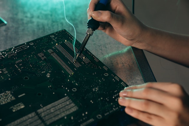
Gallium Arsenide Wafer: A Key Component in Electronic Device Manufacturing
The intricate crafting procedure of gallium arsenide devices holds an essential presence in the realm of device manufacturing. This compound semiconductor, a concoction resulting from the fusion of elements gallium and arsenic, possesses qualities that earmark it as a material par excellence for sculpting high-performance devices. The properties inherent to gallium arsenide encompass a lofty refractive index and thermal conductivity which overshadows silicon-based contraptions. These distinct traits empower GaAs-based mechanisms to function at augmented frequencies thereby suiting them aptly for applications such as Monolithic Microwave Integrated Circuits (MMICs) or RF power amplifiers.
The epitaxy technique weaves its significance into the formation of GaAs wafers. This approach involves depositing strata of materials with divergent properties onto the wafer surface, offering precise mastery over physical attributes and electronic demeanor of semiconductor gadgets. A primary feature includes its dielectric constant being approximately 0.2 lower than what is observed in silicon counterparts, this contributes to superior performance under high-frequency circumstances. Moreover, integrating phosphide into Gallium Arsenide during this process culminates in enhanced resilience against electrical breakdown – a frequent concern encountered by numerous other semiconductors.
Gallium Arsenide also maintains substantial relevance within solar energy technology courtesy its efficiency when employed in photovoltaic cells compared to conventional silicon cells. The intrinsic properties of GaAs like its wide bandgap and low defect density capacitate these solar cells to perform impressively even amidst dim light conditions – thereby magnifying overall energy productivity substantially beyond what traditional methods can proffer.
The Importance of Gallium Arsenide in Solar Cells Production
The crucial significance of Gallium Arsenide (GaAs) in the manufacturing of solar cells is attributed to its distinctive characteristics. As a compound comprising two elements, gallium and arsenic, GaAs operates as an essential III-V semiconductor. It possesses a Zinc Blende crystal structure – often referred to as GaAs crystal.
What sets it apart in the realm of materials science and engineering, particularly for solar panels, is its direct band gap attribute. This feature enhances its ability to absorb light proficiently which renders it suitable for photovoltaic applications like silicon-based solar devices.
Unlike commonplace silicon wafers utilized in CMOS technology, GaAs offers superior functionality at high frequencies. With this material at their core, devices can operate effectively up to 250 GHz frequency range – a feat unreachable with conventional silicon-based semiconductors. Devices such as laser diodes and monolithic microwave integrated circuits (MMICs), along with other gadgets like microwaves frequently used in RF industry stand out due to their need for device isolation at higher frequencies.
The process of chemical vapor deposition serves notably within semiconductor fabrication when integrating GaAS into circuit design; primarily through crafting an SiO layer on top of the substrate prior to depositation of active layers using this method. The technique guarantees high-grade outcomes by curbing defects within these layers resulting in enhanced device performance compared to Silicon counterparts.
Moreover, GaAS possesses elevated electron mobility that speeds up operations while reducing power consumption more than traditional methods making them ideal from consumer electronics all the way till advanced military systems thus underscoring their relevance across multiple sectors.
Incorporating GaAs-Based Devices in Circuit Design
Immersed in the complex universe of circuit design and manufacturing, Gallium Arsenide (GaAs) has surfaced as an esteemed semiconductor material due to its distinctive attributes. Endowed with a remarkable resistance to radiation damage, GaAs shows particular promise for applications in the cosmos where cosmic rays are unavoidable guests. Its high electron mobility paves way for intricate designs without any compromise on operational efficiency.
The energy band structure of GaAs is another feather in its cap, boasting superior conductivity over conventional silicon circuits – this advantage translates into quicker device operation.
Incepting production of devices based on GaAs involves commencing from a single slice or ‘wafer’ of it. Over this wafer’s expanse, multiple identical circuits spring up through processes like photolithography and etching. The quality of the wafer’s surface isn’t just ornamental but plays a pivotal role – premium quality ensures minimal defects during these stages. Yield optimization across the wafer can drastically cut down manufacturing expenses; this aspect is shaped by both design considerations and control over fabrication parameters.
Integration of first GaAS heterostructure into circuit designs demands comprehension not merely about electrical characteristics but also thermal ones since they shape what is known as ‘GaAS power’ or power handling capacity. This understanding enhances optimal utilization of inherent benefits like radiation damage resistance and superior conductivity that outshines other materials such as Silicon.
Through vigilant management at every phase from conception to completion, each component’s performance can be optimized within its broader system environment while keeping overall production costs under check – all these points are depicted clearly in an illustrative figure (not provided).

Comments are closed.