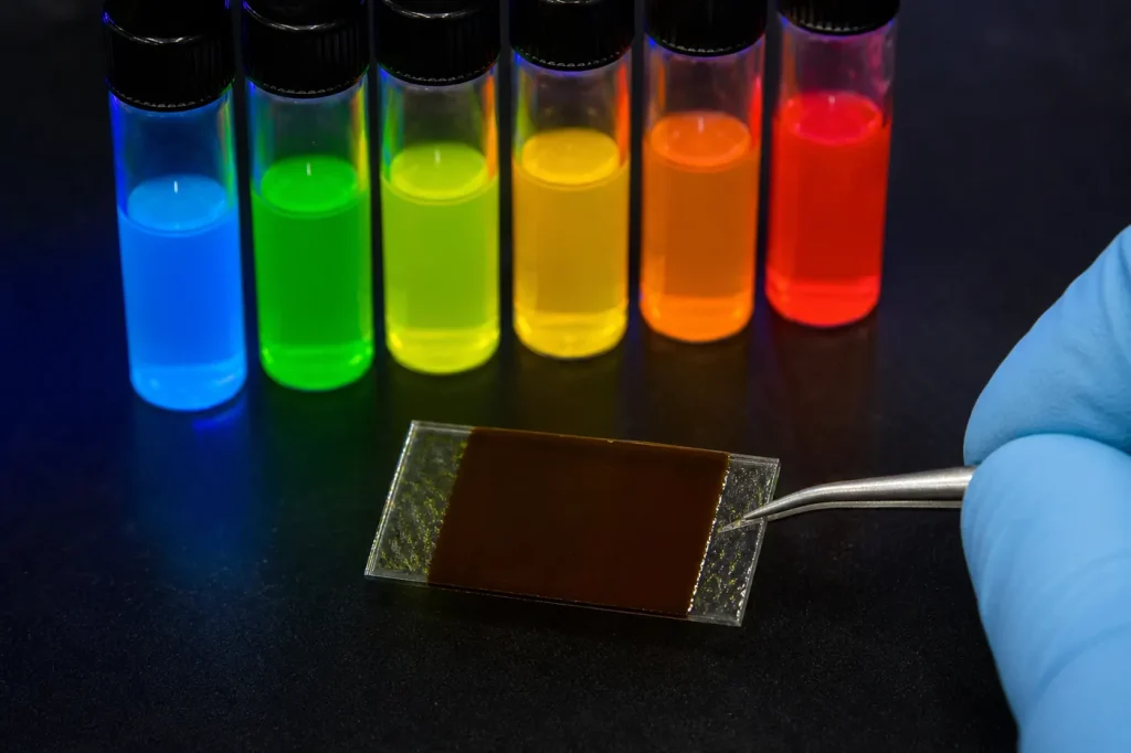
Perovskites, quantum dots and nanomaterials are semiconductors whose behaviour is set by crystal structure or size as much as by composition. Halide perovskites are ABX3 crystals that absorb sunlight strongly. Quantum dots are nanocrystals whose bandgap depends on their diameter. Carbon nanotubes are rolled-up graphene. Start here for each class and its commercial status.
Key numbers at 300 K
These are families, not single materials. Values depend on the specific composition, size and processing, so treat the figures as typical ranges.
| Material | Class | Bandgap (eV) | Tuned by | Commercial status |
|---|---|---|---|---|
| MAPbI3 (methylammonium lead iodide) | Hybrid halide perovskite | ~1.55–1.6 (direct) | Halide and cation mix; about 1.2–3 eV across the family | Pilot lines and early modules; stability is the hurdle |
| CsPbBr3 | All-inorganic halide perovskite | ~2.3 (direct) | Halide mix and nanocrystal size | Research, mainly as light emitters |
| CdSe quantum dots | II-VI nanocrystal | 1.74 bulk; wider in dots | Diameter, roughly 2–7 nm for visible emission | Display colour converters; cadmium is restricted in some markets |
| InP quantum dots | III-V nanocrystal | 1.34 bulk; wider in dots | Diameter and shell | Cadmium-free colour converters in commercial displays |
| PbS quantum dots | IV-VI nanocrystal | 0.41 bulk; wider in dots | Diameter | Short-wave infrared photodetectors and image sensors |
| Semiconducting single-wall carbon nanotubes | 1D carbon | ~0.4–0.8 for 1–2 nm diameters | Chirality and diameter (Eg ≈ 0.8 eV·nm / d) | Transistors in research; nanotubes in general are sold as conductive additives |
| Metal-organic frameworks (MOFs) | Porous metal-organic crystals | Mostly insulating; a few conductive MOFs | Choice of metal and organic linker | Early commercial in gas storage and separation; electronics in research |
| Si (reference) | Bulk semiconductor | 1.12 (indirect) | Doping only | Mature |
What is a perovskite semiconductor?
A perovskite is any crystal with the ABX3 structure of the mineral CaTiO3. In solar-cell perovskites, A is a cation such as methylammonium, formamidinium or caesium, B is lead or tin, and X is a halide: iodide, bromide or chloride. Swapping these ions tunes the bandgap continuously, which few other semiconductors allow.
Three traits have made halide perovskites one of the most studied solar materials since 2009. They absorb light so strongly that a film under a micrometre thick captures most visible sunlight, against well over 100 µm for a crystalline silicon wafer. They tolerate defects that would cripple silicon. And they can be coated from solution at low temperature. The first perovskite solar cell, reported in 2009, converted 3.8% of sunlight (Kojima et al., JACS). Lab single-junction cells now reach efficiencies comparable to crystalline silicon cells, and perovskite-silicon tandems have passed the best single-junction silicon cells. Check the NREL Best Research-Cell Efficiency Chart for current certified figures. Read hybrid perovskites for solar cells and perovskites in solar cells and optoelectronics.
What holds perovskites back?
Stability. Moisture, heat, oxygen and light all degrade halide perovskites, and mobile ions in the crystal drift under electric fields, which slowly changes device behaviour. The best-performing compositions contain lead, so modules need encapsulation that prevents leakage and a plan for recycling. Tin-based alternatives avoid lead but oxidize easily.
The nearest-term route to market is the tandem cell. A wide-gap perovskite layer on top absorbs blue and green light, and a silicon cell underneath absorbs the red and infrared light that passes through. Each material handles the part of the spectrum it converts best, so the stack beats either cell alone. That plays to silicon’s existing supply chain rather than replacing it.
What are quantum dots made of?
Quantum dots are semiconductor nanocrystals, typically 2–10 nm across. Common cores are CdSe, InP, PbS and perovskite compositions such as CsPbBr3, and most commercial dots add a wider-gap shell such as ZnS or ZnSe to protect the surface and raise brightness.
Their colour comes from quantum confinement. When a crystal is smaller than its exciton Bohr radius (the natural size of a bound electron-hole pair, about 5–6 nm in CdSe), the bandgap widens as the dot shrinks (Brus, 1984). Small dots glow blue, larger dots glow red, from the same material. See our quantum dots guide.
Are carbon nanotubes semiconductors?
Some are. A single-wall carbon nanotube is a sheet of graphene rolled into a closed cylinder, and the angle of the roll, called chirality and written as indices (n, m), decides its electronic type. If n − m is divisible by 3, the tube is metallic. Otherwise it is semiconducting, with a gap of roughly 0.8 eV divided by the diameter in nanometres. Random growth yields about one-third metallic tubes, so sorting and placement remain the main obstacles for nanotube transistors. See carbon nanotubes in electronics and energy storage. Metal-organic frameworks, covered in our MOFs guide, are mostly insulating porous crystals used for sensing and storage.
Which of these are commercial today?
- Quantum dots: yes. They are used as colour converters in commercial displays, with cadmium-free InP dots common because of cadmium restrictions.
- Carbon nanotubes: yes as bulk additives, for example conductive agents in battery electrodes. Semiconducting nanotube electronics are still in research.
- Halide perovskites: moving from lab to pilot production and early modules. Long-term field stability is still being proven.
- MOFs: early commercial use in gas storage and separation, not in electronics.
For the conventional crystalline materials these classes are measured against, see what a compound semiconductor is, III-V semiconductors and wide-bandgap semiconductors.
Start here
- Harnessing the Power of the Sun: Hybrid Organic-Inorganic Perovskites for High-Efficiency Solar Cells
- Quantum Dots: Revolutionizing Display Technology and Lighting Applications
- Powering the Future: The Role of Carbon Nanotubes (CNTs) in Electronics and Energy Storage
- Understanding the Basics of Compound Semiconductors
All perovskite, quantum dot and nanomaterial guides
Perovskites
- Harnessing the Power of the Sun: Hybrid Organic-Inorganic Perovskites for High-Efficiency Solar Cells
- Harnessing the Sun: Perovskite Materials Pioneering the Future of Solar Cells and Optoelectronics
Quantum dots and nanomaterials
- Quantum Dots: Revolutionizing Display Technology and Lighting Applications
- Powering the Future: The Role of Carbon Nanotubes (CNTs) in Electronics and Energy Storage
- Metal-Organic Frameworks (MOFs): The Future of Gas Sensing and Energy Storage Technologies
Semiconductor fundamentals
- Understanding the Basics of Compound Semiconductors
- What is a Compound Semiconductor
- What Are III-V Semiconductors? Members, Properties and Uses
- What Is a Wide-Bandgap Semiconductor?
- Semiconductors Examples
Quick answers
- What materials are semiconductors?
- What are types of semiconductor?
- What is a semiconductor made of?
- What are examples of compound semiconductors?
- What are the advantages of compound semiconductors?
Related hubs
- All materials
- Organic semiconductors
- 2D semiconductors
- Silicon and germanium
- Semiconductor comparisons
Frequently asked questions
Why do smaller quantum dots emit bluer light?
Squeezing the electron and hole into a smaller crystal raises their confinement energy, which widens the effective bandgap. A wider gap means higher-energy photons, which are bluer.
Are perovskite solar cells for sale?
Early perovskite and perovskite-silicon tandem modules are in pilot production. They are not yet a mainstream product, mainly because long-term outdoor stability is still being demonstrated.
Are quantum dots toxic?
It depends on the core. CdSe and PbS contain toxic heavy metals and are regulated in some markets. InP dots are the main cadmium-free option for displays, and carbon and silicon dots are studied as lower-toxicity alternatives.
Sources
- National Renewable Energy Laboratory (NREL), Best Research-Cell Efficiency Chart. https://www.nrel.gov/pv/cell-efficiency.html
- L. E. Brus, “Electron-electron and electron-hole interactions in small semiconductor crystallites: the size dependence of the lowest excited electronic state,” Journal of Chemical Physics 80, 4403 (1984).
- R. Saito, G. Dresselhaus and M. S. Dresselhaus, Physical Properties of Carbon Nanotubes, Imperial College Press (1998).
- O. Madelung, Semiconductors: Data Handbook, 3rd ed., Springer (2004), with the Ioffe Institute NSM archive for InP and Si. http://www.ioffe.ru/SVA/NSM/Semicond/
