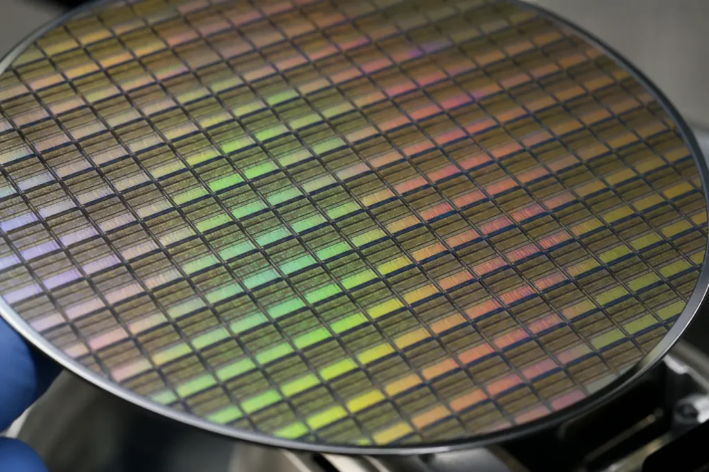
Gallium nitride (GaN) is a III-nitride, wide-bandgap compound semiconductor with a direct bandgap of 3.39 eV at 300 K. That gap, a critical field about ten times silicon’s and a high-mobility electron channel make GaN the material behind blue and white LEDs, radar and base-station amplifiers, and compact fast chargers.
Key takeaways
- Bandgap 3.39 eV (direct), critical field about 3.3 MV/cm, versus 1.12 eV and about 0.3 MV/cm for silicon.
- The AlGaN/GaN two-dimensional electron gas reaches about 1,500 to 2,000 cm²/V·s with no doping, which is why GaN transistors switch fast.
- GaN is mostly grown on silicon, SiC or sapphire, because native GaN wafers are small and costly.
- Sweet spot: 650 V and below for power, high-power RF, and blue, green and UV light.
Key numbers at 300 K
Values are for wurtzite GaN, the stable crystal form, at 300 K. Silicon is shown as the baseline. Where published values spread, a range is given.
| Property (300 K) | GaN (wurtzite) | Si (reference) |
|---|---|---|
| Crystal structure | Wurtzite (hexagonal) | Diamond cubic |
| Lattice constant (Å) | a = 3.189, c = 5.185 | 5.431 |
| Bandgap (eV) | 3.39, direct | 1.12, indirect |
| Electron mobility, bulk (cm²/V·s) | Up to about 1,000 | About 1,400 |
| Electron mobility, AlGaN/GaN 2DEG (cm²/V·s) | About 1,500 to 2,000 | — |
| Hole mobility (cm²/V·s) | Up to about 200 | About 450 |
| Critical field (MV/cm) | About 3.3 (reported 3 to 5) | About 0.3 |
| Saturation velocity (107 cm/s) | About 2.5 | About 1.0 |
| Thermal conductivity (W/m·K) | About 130 to 230 | About 150 |
| Static dielectric constant | About 8.9 | 11.7 |
| Density (g/cm³) | 6.15 | 2.33 |
What is gallium nitride?
GaN is a compound of gallium (group III) and nitrogen (group V). It belongs to the III-nitride family with aluminium nitride (AlN, about 6.2 eV) and indium nitride (InN, about 0.7 eV). Alloys of the three, AlGaN and InGaN, can in principle be tuned from deep ultraviolet to near-infrared. That tunability is rare, and it is why one material family covers LEDs, lasers and transistors.
Commercial GaN began with blue LEDs in the 1990s, work recognised by the 2014 Nobel Prize in Physics. Power and RF transistors followed. Our history piece, Gallium Nitride (GaN): The Emergent Force in Semiconductor Technology, traces that path. For where GaN sits among other compounds, see III-V semiconductors.
What are the key properties of GaN?
Two properties do most of the work. First, the critical field of about 3.3 MV/cm lets a device block a given voltage with a drift region roughly a tenth as thick as silicon’s. Second, GaN’s crystal is polar. When a thin AlGaN layer sits on GaN, the polarisation mismatch pulls electrons into a sheet at the interface: the two-dimensional electron gas (2DEG). It needs no doping, so electrons scatter less and mobility reaches about 1,500 to 2,000 cm²/V·s.
A transistor built on that sheet is a high-electron-mobility transistor (HEMT). High mobility plus high field gives low on-resistance in a small die, and a small die has low capacitance and fast switching. The weak spot is heat: GaN conducts heat about as well as silicon, well below SiC. The full data set is in the GaN properties table, and the wide-bandgap guide explains why bandgap drives critical field.
What is GaN used for?
Power conversion. GaN HEMTs rated about 100 V to 650 V run USB-C chargers, data-centre power supplies and motor drives. Higher switching frequency shrinks the magnetics, which is where the size saving comes from. See GaN in high-power applications.
RF. GaN-on-SiC HEMTs deliver high output power per millimetre of gate at microwave frequencies, so they are used in radar, satellite links and cellular base stations. Light. InGaN quantum wells make blue and green LEDs; a blue LED plus a yellow phosphor makes white light. AlGaN extends emission into the ultraviolet, including UV-C for disinfection, covered in our article on nitride UV LEDs.
Why is GaN grown on foreign substrates?
Bulk GaN crystals are hard to grow, so native GaN wafers are small and expensive. Most GaN is grown as a thin epitaxial film on another wafer. Each choice trades cost against crystal quality and heat removal. Silicon is cheapest, comes in large diameters and runs in existing fabs, but its lattice mismatch with GaN is about 17%, so thick buffer layers are needed. SiC mismatches by only about 3.5% and removes heat best, which suits RF. Sapphire is cheap and insulating, the long-time LED standard. Native GaN gives the lowest defect density, for lasers and vertical power devices.
The film itself is grown by metal-organic chemical vapour deposition (MOCVD), which reacts trimethylgallium with ammonia at around 1,000 °C. Molecular beam epitaxy is used for some RF structures. Native bulk crystals come from hydride vapour phase epitaxy (HVPE) or ammonothermal growth, both slow. Mismatched growth leaves threading dislocations, line defects that run up through the film, and their density sets LED efficiency and transistor reliability.
Our comparison GaN-on-Si vs GaN-on-SiC vs GaN-on-Sapphire vs GaN-on-GaN sets out defect densities, wafer sizes and the applications each substrate wins.
How does GaN compare with SiC and Si?
GaN and SiC have similar bandgaps near 3.3 eV and similar critical fields. GaN wins on channel mobility and switching speed. SiC wins on thermal conductivity (about 330 to 490 W/m·K), avalanche ruggedness and voltage range, because SiC devices are vertical while GaN power HEMTs are mostly lateral. Pick GaN for compact, high-frequency designs at 650 V and below. Pick SiC for 1,200 V and above. Silicon still wins on cost wherever its losses are acceptable.
Detailed head-to-heads are in our comparisons section. For the wider family context, start with the basics of compound semiconductors or go back to the materials index.
Start here
- GaN Properties Table: Bandgap, Mobility, Breakdown Field, Thermal Conductivity
- GaN-on-Si vs GaN-on-SiC vs GaN-on-Sapphire vs GaN-on-GaN
- Gallium Nitride (GaN) Semiconductors The Future of High-Power Applications
All gallium nitride guides
Properties and data
- GaN Properties Table: Bandgap, Mobility, Breakdown Field, Thermal Conductivity
- Gallium Nitride (GaN): The Emergent Force in Semiconductor Technology
Devices and applications
- Gallium Nitride (GaN) Semiconductors The Future of High-Power Applications
- Illuminating Innovations: Nitride-based Semiconductors in Ultraviolet Light-Emitting Diodes (LEDs)
Substrates and manufacturing
Compound semiconductor background
- Understanding the Basics of Compound Semiconductors
- What is a Compound Semiconductor
- What Are III-V Semiconductors? Members, Properties and Uses
- What Is a Wide-Bandgap Semiconductor?
- Semiconductors Examples
FAQs
- What materials are semiconductors?
- What are types of semiconductor?
- What are the advantages of compound semiconductors?
- What is a semiconductor made of?
- What are examples of compound semiconductors?
Related material hubs
GaN deep dives
- GaN Crystal Structure: Wurtzite, Polarity and Crystal Planes
- GaN Polarization: Spontaneous and Piezoelectric Fields Explained
- Why p-Type GaN Is Hard: Magnesium Doping and Activation
- Defects in GaN: Threading Dislocations and Their Effects
- InGaN: The Alloy Behind Blue and Green LEDs
- Semiconductor Alloys and Bandgap Engineering (InGaN, AlGaAs, InGaAsP)
Head-to-head comparisons
- GaN Properties Table: Bandgap, Mobility, Breakdown Field, Thermal Conductivity
- GaN vs SiC: Properties, Voltage Range and Which to Choose
- GaN vs Silicon: Why GaN Switches Faster and Where Si Still Wins
- GaN-on-Si vs GaN-on-SiC vs GaN-on-Sapphire vs GaN-on-GaN
- Breakdown Field of Semiconductors Compared
More GaN deep dives
- AlGaN: Barrier Layers for HEMTs and Deep-UV Emitters
- GaN Reliability: Current Collapse, Dynamic On-Resistance and Qualification
- GaN vs GaAs for RF: Power Density, Frequency and Cost
FAQ
Is GaN better than silicon?
For power conversion up to about 650 V and for high-power RF, yes: GaN has about ten times the critical field and a faster channel, so it loses less energy. Silicon remains cheaper and better for logic.
Is GaN a direct-bandgap semiconductor?
Yes. Its 3.39 eV gap is direct, which is why GaN and InGaN emit light efficiently and are used in blue, green and white LEDs and in violet lasers.
Why are GaN chargers smaller?
GaN transistors switch at higher frequency with lower loss. Higher frequency allows smaller transformers and capacitors, and lower loss means less heat sinking.
Sources
- Ioffe Institute, New Semiconductor Materials (NSM) archive, http://www.ioffe.ru/SVA/NSM/Semicond/
- U. K. Mishra, P. Parikh and Y.-F. Wu, “AlGaN/GaN HEMTs: an overview of device operation and applications,” Proceedings of the IEEE (2002).
- S. M. Sze and K. K. Ng, Physics of Semiconductor Devices, 3rd ed., Wiley.
