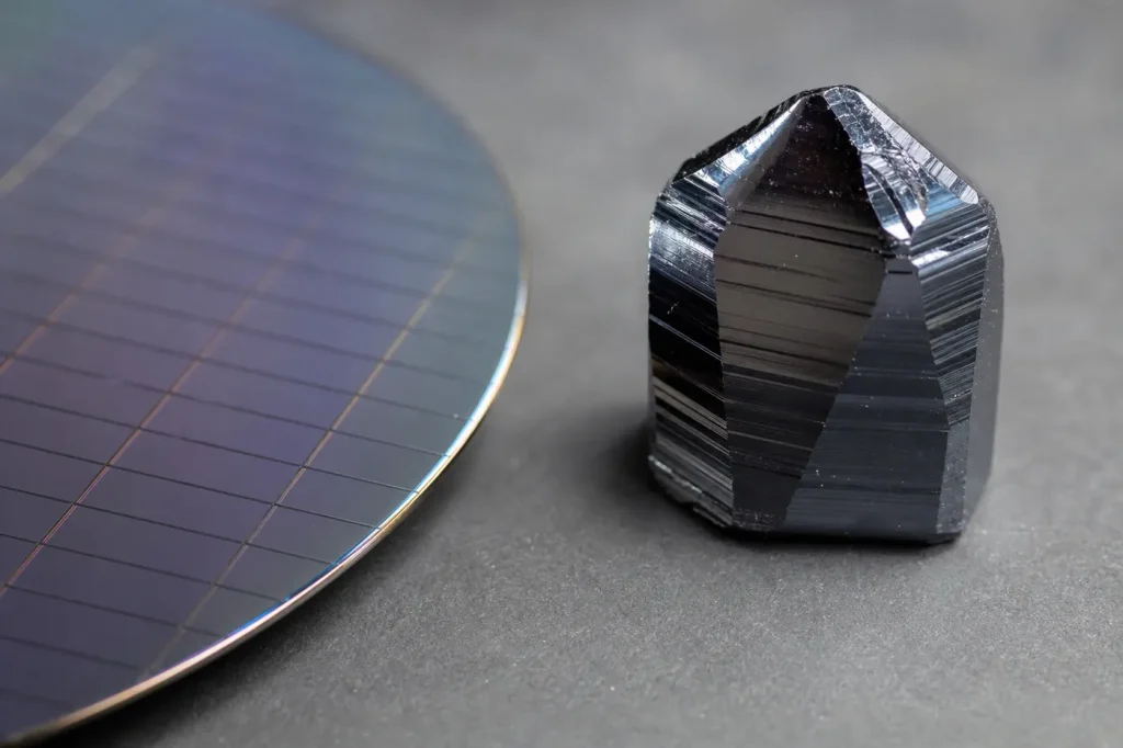
Silicon and germanium are the group IV elemental semiconductors: single elements that crystallize in the diamond-cubic structure, both with an indirect bandgap. Silicon (1.12 eV) is the baseline every other material is measured against. Germanium (0.66 eV) trades a narrower gap for higher mobility. Start here for their properties, SiGe alloys and where compounds beat them.
Key numbers at 300 K
| Property (300 K) | Silicon (Si) | Germanium (Ge) | What it means |
|---|---|---|---|
| Bandgap (eV) | 1.12 (indirect) | 0.66 (indirect) | Ge leaks more current and tolerates less heat |
| Lowest direct gap (eV) | ~3.4 | ~0.8 | Ge’s 0.8 eV direct gap absorbs 1.55 µm telecom light |
| Electron mobility (cm²/V·s) | ≤1,400 | ≤3,900 | Ge electrons move about 2.8 times faster |
| Hole mobility (cm²/V·s) | ≤450 | ≤1,900 | Ge holes are about 4 times faster, the best of any common semiconductor |
| Critical field (MV/cm) | ~0.3 | ~0.1 | Neither suits high-voltage power |
| Thermal conductivity (W/m·K) | 130–150 | ~58 | Silicon spreads heat more than twice as well |
| Relative permittivity | 11.7 | 16.2 | Sets junction and gate capacitance |
| Lattice constant (Å) | 5.431 | 5.658 | About 4.2% mismatch, the source of strain in SiGe |
| Intrinsic carrier density (cm−3) | ~1 × 10¹⁰ | ~2 × 10¹³ | Ge’s narrow gap gives about 2,000 times more thermal carriers |
| Melting point (°C) | 1,412 | 937 | Both grown as large single crystals by the Czochralski method |
| Native oxide | SiO2, stable and insulating | GeO2, water-soluble and unstable | The single biggest reason silicon won |
Why is silicon the baseline semiconductor?
Silicon is not the best at any single property. It wins on the combination. Its 1.12 eV gap is wide enough to keep leakage low at normal operating temperatures. It grows a native oxide, SiO2, that is a near-ideal insulator with a clean interface, which made the MOSFET and the planar process possible. It is the second most abundant element in Earth’s crust, and it can be grown as near-perfect single crystals and sliced into 300 mm wafers.
Decades of process investment compound those advantages. That is why every other material on this site is judged by how it compares with silicon on cost, wafer size and yield. Read why silicon dominates, the silicon crystal structure guide, and how silicon transistors power computer processors.
How does germanium differ from silicon?
Germanium came first. The point-contact transistor demonstrated at Bell Labs in 1947 used germanium, and early transistor radios ran on it. Its narrow 0.66 eV gap was the problem. Germanium devices leak more current, and the leakage climbs quickly with temperature. Its oxide dissolves in water, so it could not support the planar process. Silicon took over through the late 1950s and 1960s.
Germanium never disappeared. Its hole mobility is about four times silicon’s, its direct gap near 0.8 eV absorbs near-infrared light, and its lattice constant almost matches GaAs (5.653 Å). Those three facts explain where it is used today. See the germanium basics, the full germanium properties guide and its discovery and history. Mendeleev predicted the element as “eka-silicon” before Clemens Winkler isolated it in 1886.
Why can’t silicon emit light efficiently?
Both silicon and germanium have an indirect bandgap. The lowest-energy electrons in the conduction band sit at a different crystal momentum from the highest-energy holes in the valence band. To recombine and emit a photon, an electron also needs a lattice vibration (a phonon) to make up the momentum difference. That three-body process is slow, so electrons usually lose their energy as heat first.
The consequence is practical. LEDs and lasers are made from direct-gap compounds such as GaAs, InP and GaN, not silicon. Silicon still absorbs light well up to a wavelength of about 1.1 µm, which is why it dominates solar cells and image sensors. In silicon photonics, silicon carries light in waveguides, germanium detects it, and III-V lasers are bonded on to supply it. Read about silicon photonics, germanium in optoelectronics, the fundamentals of solar cells and silicon solar cells.
What is SiGe?
Silicon-germanium (Si1−xGex) is an alloy of the two elements in any ratio, where x is the germanium fraction. Because the two lattices differ by about 4.2%, a thin SiGe layer grown on silicon is compressed, and that strain changes its band structure. The bandgap shrinks as germanium content rises, moving from silicon’s value toward germanium’s.
Engineers use it in three ways. SiGe heterojunction bipolar transistors (HBTs) use a graded SiGe base to speed up electrons, which serves RF and high-speed analog circuits. SiGe source and drain regions strain silicon channels to raise hole mobility in CMOS logic. Silicon/SiGe heterostructures are also a platform for spin-qubit research, covered in our silicon quantum dots guide. Germanium wafers, meanwhile, serve as substrates for III-V multi-junction space solar cells. More in germanium in devices and silicon nanowires.
Where do compound semiconductors beat silicon?
In three places, each tied to one property. Direct-gap III-V compounds emit light efficiently. GaAs and InP carry electrons four to six times faster for RF and high-speed links. SiC and GaN have critical fields 7 to 11 times silicon’s, which shrinks power devices. Everywhere else, silicon’s cost and maturity usually win. Start with what a compound semiconductor is, then III-V semiconductors and wide-bandgap semiconductors. For side-by-side numbers, including Si vs Ge and SiC vs Si, see semiconductor comparisons and the SiC hub.
Start here
- Silicon: The Superhero of Semiconductors Unveiled
- Understanding the Properties of Germanium as a Semiconductor Material
- What is a Compound Semiconductor
- What Is a Wide-Bandgap Semiconductor?
All silicon and germanium guides
Silicon fundamentals
- Silicon: The Superhero of Semiconductors Unveiled
- The Intricacies of Silicon Crystal Structure: Unleashing the Power of Semiconductors
- The Silicon Powerhouse: How Semiconductors Drive Our Computer Processors
- The Silicon Symphony: Transistors Powering the Electronics Orchestra
Silicon in solar, photonics and quantum devices
- Understanding the Fundamentals of Solar Cell Technology
- Sunlight: Silicon Solar Cells and their Powerful Role in Renewable Energy
- The Luminous Leap: Silicon Photonics Revolutionizing Optical Communications
- Treading the Nanoworld: Silicon Nanowires and Their Promising Role in Future Semiconductor Devices
- Quantum Leap with Silicon: Exploring Silicon Quantum Dots in the Realm of Quantum Computing
Germanium
- Understanding the Basics of Germanium as a Semiconductor
- Understanding the Properties of Germanium as a Semiconductor Material
- Understanding the Elemental Structure of Germanium
- The Discovery and History of Germanium
- Germanium: A Comprehensive Overview
- Evolving Role of Germanium in the Global Semiconductor Arena
- The Role of Germanium in Semiconductor Devices
- Understanding the Role of Germanium in Optoelectronic Devices
Beyond silicon: compound semiconductors
- Understanding the Basics of Compound Semiconductors
- What is a Compound Semiconductor
- What Are III-V Semiconductors? Members, Properties and Uses
- What Is a Wide-Bandgap Semiconductor?
- Semiconductors Examples
Quick answers
- What materials are semiconductors?
- What are types of semiconductor?
- What is a semiconductor made of?
- What are examples of compound semiconductors?
- What are the advantages of compound semiconductors?
Frequently asked questions
Is germanium better than silicon?
Only on mobility and infrared absorption. Germanium’s electrons and holes move about 2.8 and 4 times faster, but its 0.66 eV gap leaks more, its oxide is unstable and its thermal conductivity is less than half of silicon’s. It is used where those strengths count, not as a general replacement.
Can silicon make LEDs or lasers?
Not efficiently. Its indirect bandgap makes light emission slow compared with heat loss. Practical silicon photonics bonds III-V lasers onto silicon chips and uses germanium photodetectors.
What is the bandgap of SiGe?
It depends on the germanium fraction and on strain. It moves from silicon’s 1.12 eV toward germanium’s 0.66 eV as germanium content rises, and compressive strain on a silicon substrate lowers it further.
Sources
- Ioffe Institute, New Semiconductor Materials (NSM) archive: Si and Ge property pages. http://www.ioffe.ru/SVA/NSM/Semicond/
- S. M. Sze and K. K. Ng, Physics of Semiconductor Devices, 3rd ed., Wiley (band structure, oxides, HBTs).
- R. F. Pierret, Semiconductor Device Fundamentals, Addison-Wesley (indirect-gap recombination, intrinsic carrier density).
