Gallium arsenide (GaAs) is a III-V compound semiconductor with a direct bandgap of 1.42 eV at 300 K and electron mobility up to about 8,500 cm²/V·s, roughly six times silicon’s. Those two numbers explain its uses: RF amplifiers and switches in phones, infrared lasers and VCSELs, and high-efficiency solar cells.
Key takeaways
- Bandgap 1.42 eV, direct, so GaAs emits near-infrared light at about 870 nm.
- Electron mobility up to about 8,500 cm²/V·s against about 1,400 for silicon; hole mobility is no better than silicon’s.
- Main device families: pHEMTs, HBTs, VCSELs and multi-junction solar cells.
- GaN has taken high-power RF, but GaAs still dominates low-voltage handset front ends.
Key numbers at 300 K
Values are for undoped GaAs at 300 K, with silicon as the baseline. Mobility figures are upper limits for pure material; doping lowers them.
| Property (300 K) | GaAs | Si (reference) |
|---|---|---|
| Crystal structure | Zincblende (cubic) | Diamond cubic |
| Lattice constant (Å) | 5.653 | 5.431 |
| Bandgap (eV) | 1.42, direct | 1.12, indirect |
| Electron mobility (cm²/V·s) | Up to about 8,500 | About 1,400 |
| Hole mobility (cm²/V·s) | Up to about 400 | About 450 |
| Electron effective mass (m0) | 0.063 | About 0.26 (conductivity mass) |
| Critical field (MV/cm) | About 0.4 | About 0.3 |
| Thermal conductivity (W/m·K) | About 55 | About 150 |
| Static dielectric constant | 12.9 | 11.7 |
| Intrinsic carrier concentration (cm-3) | About 2 × 10⁶ | About 1 × 10¹⁰ |
| Density (g/cm³) | 5.32 | 2.33 |
What is gallium arsenide?
GaAs pairs gallium from group III with arsenic from group V in a zincblende crystal, the same cubic frame as silicon’s diamond lattice but with two alternating atom types. Its gap is direct, so electrons and holes recombine by emitting light. GaAs can also be made semi-insulating, with resistivity around 107 to 108 Ω·cm, which isolates devices on the same chip and cuts parasitic capacitance at microwave frequencies.
For the basics, see what GaAs is, its composition and crystal structure and how GaAs is classified. Its place in the wider family is covered in III-V semiconductors.
Why does GaAs have higher electron mobility than Si?
Mobility measures how fast a carrier drifts in a given field. In GaAs the lowest conduction-band valley is sharply curved, which gives electrons a small effective mass of 0.063 m0, about a quarter of silicon’s conductivity mass. Lighter electrons accelerate more between collisions. The result is electron mobility up to about 8,500 cm²/V·s against about 1,400 for silicon.
The advantage is one-sided. Hole mobility is no better than silicon’s, which rules out efficient complementary logic. GaAs has no stable native oxide, unlike silicon’s SiO2, and conducts heat about a third as well. That is why GaAs never displaced silicon for computing. Full data is in the properties of gallium arsenide.
What is GaAs used for?
Four device families carry the volume. The pHEMT (pseudomorphic high-electron-mobility transistor, with a strained InGaAs channel) serves RF switches and low-noise amplifiers. The HBT (heterojunction bipolar transistor, usually InGaP/GaAs) is the standard power amplifier in phones. The VCSEL (vertical-cavity surface-emitting laser) at about 850 nm and 940 nm drives short-reach data links and 3D sensing. Solar cells on GaAs reach the highest single-junction efficiencies, near 29%, and multi-junction GaAs-based cells power most satellites.
See GaAs in microwave devices, GaAs in solar technology and the broader GaAs applications overview.
Is GaN replacing GaAs in RF?
In high-power RF, largely yes. GaN has a critical field near 3.3 MV/cm against about 0.4 MV/cm for GaAs, so it runs at much higher drain voltage and delivers several times the power per millimetre of gate. Radar, satellite and base-station amplifiers have moved to GaN-on-SiC.
In phones, no. Handset power amplifiers run from a battery of a few volts, where GaN’s voltage headroom adds little, and GaAs HBTs offer mature linearity, yield and cost on 150 mm wafers. GaAs also keeps VCSELs, which GaN cannot make at those wavelengths. The trade-offs are covered in our comparisons section.
How is GaAs made?
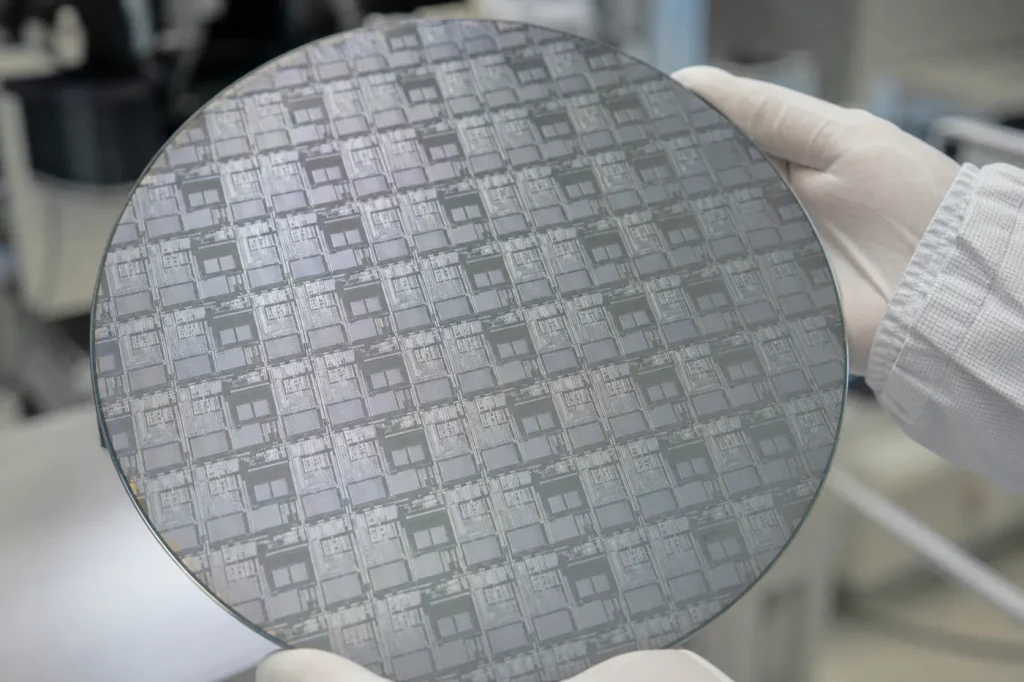
Bulk crystals are grown from a melt at about 1,240 °C. Arsenic boils off far below that temperature, so the melt must be contained. In liquid-encapsulated Czochralski (LEC) growth, a layer of molten boron oxide caps the melt while a seed pulls the crystal upward. In vertical gradient freeze (VGF), the melt solidifies slowly from the bottom of a sealed crucible, which gives lower dislocation density. RF wafers are mostly 150 mm, against 300 mm for silicon.
Device layers are then grown by MOCVD or molecular beam epitaxy (MBE), which deposit atomic layers of GaAs, AlGaAs, InGaP and InGaAs with abrupt interfaces. Those interfaces make HEMTs, HBTs and VCSEL mirrors possible. AlGaAs is the key partner: its lattice almost matches GaAs across all compositions, so designers can stack layers of different bandgap without strain.
How does GaAs compare with silicon and InP?
Against silicon, GaAs trades cost and integration density for speed and light. Pick GaAs when the job is an RF front end, an infrared emitter or a solar cell where efficiency per gram matters, as in space. Pick silicon, or SiGe for RF on a silicon line, when cost and integration come first. Against InP, GaAs has faster electrons and cheaper wafers, but cannot reach the 1.3 µm and 1.55 µm telecom wavelengths. For all materials side by side, see the materials index.
Start here
- Understanding the Basics of Gallium Arsenide (GaAs)
- Understanding the Properties of Gallium Arsenide
- Understanding GaAs: A Key Component in Microwave Semiconductor Devices
All gallium arsenide guides
Basics and properties
- Understanding the Basics of Gallium Arsenide (GaAs)
- Understanding the Properties of Gallium Arsenide
- Understanding the Composition and Function of GaAs
- Is gallium arsenide a semiconductor?
Devices and applications
- Understanding Gallium Arsenide: A Detailed Look at its Properties and Applications
- Understanding GaAs: A Key Component in Microwave Semiconductor Devices
- Understanding the Role of GaAs in Solar Technology
Compound semiconductor background
- Understanding the Basics of Compound Semiconductors
- What is a Compound Semiconductor
- What Are III-V Semiconductors? Members, Properties and Uses
- What Is a Wide-Bandgap Semiconductor?
- Semiconductors Examples
FAQs
- What materials are semiconductors?
- What are types of semiconductor?
- What are the advantages of compound semiconductors?
- What is a semiconductor made of?
- What are examples of compound semiconductors?
Related material hubs
- Semiconductor materials index
- Gallium nitride (GaN)
- Indium phosphide (InP)
- Silicon-germanium (SiGe)
- Material comparisons
GaAs deep dives
- GaAs Wafers: Semi-Insulating vs Conductive, VGF vs LEC
- AlGaAs/GaAs Heterostructures: Lattice Matching and Band Offsets
- GaN vs GaAs for RF: Power Density, Frequency and Cost
FAQ
Is GaAs better than silicon?
For RF and light emission, yes: it has higher electron mobility and a direct gap. For logic, memory and anything cost-driven, silicon wins on oxide quality, hole mobility, thermal conductivity and wafer size.
Is gallium arsenide toxic?
Solid GaAs is stable, but arsenic compounds are toxic. Fabs control dust from grinding and polishing, and the arsine gas used in epitaxy is highly toxic and tightly regulated.
Why aren’t processors made from GaAs?
GaAs lacks a good native oxide and fast holes, so dense complementary logic like silicon CMOS is impractical. Its wafers are also smaller and more expensive.
Sources
- Ioffe Institute, New Semiconductor Materials (NSM) archive, http://www.ioffe.ru/SVA/NSM/Semicond/
- S. M. Sze and K. K. Ng, Physics of Semiconductor Devices, 3rd ed., Wiley.
- S. Adachi, GaAs and Related Materials: Bulk Semiconducting and Superlattice Properties, World Scientific.
