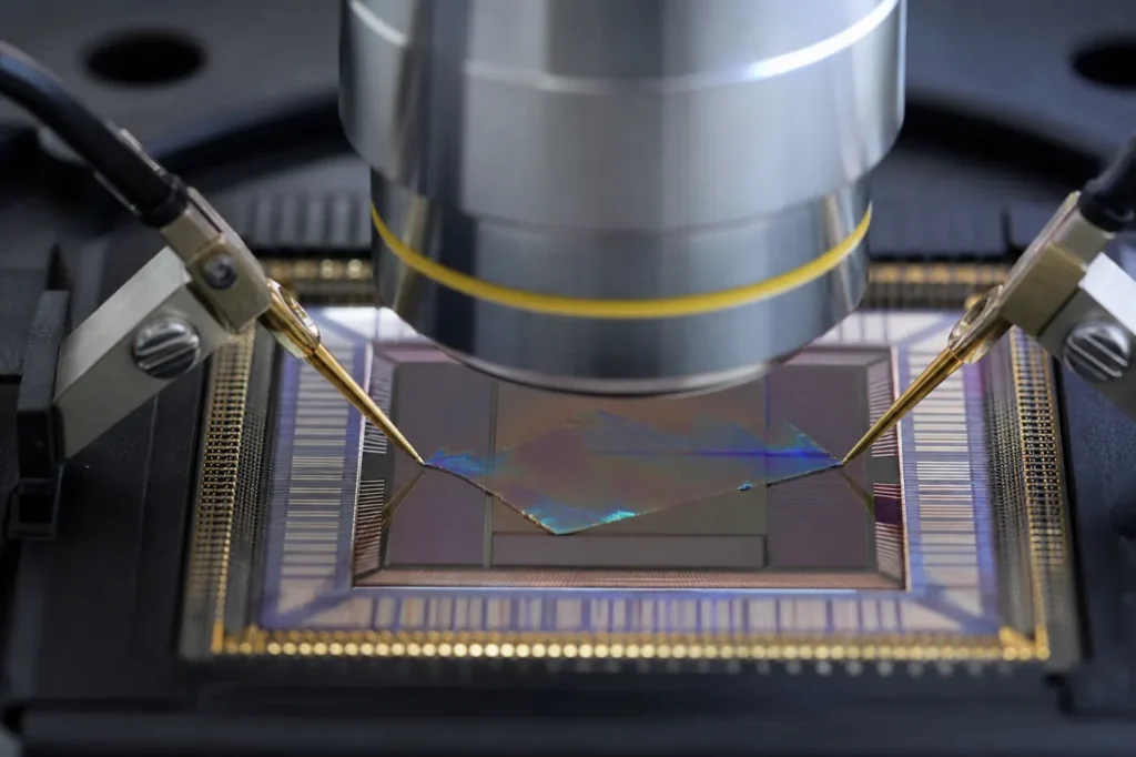
2D semiconductors are crystals only one or a few atomic layers thick, peeled or grown from layered materials. The family spans a semimetal (graphene), true semiconductors (transition metal dichalcogenides such as MoS2 and WSe2) and a wide-gap insulator (hBN). Start here for their bandgaps, mobilities and the case for replacing silicon channels.
Key numbers at 300 K
2D values depend heavily on sample quality, substrate and contacts. The figures below are typical literature ranges, not guaranteed device numbers. Silicon is included as the reference.
| Material | Class | Monolayer bandgap (eV) | Bulk bandgap (eV) | Room-temperature mobility (cm²/V·s) | Monolayer thickness (nm) |
|---|---|---|---|---|---|
| Graphene | Semimetal | 0 (no gap) | 0 (graphite) | ~10,000 on SiO2; higher on hBN | ~0.34 |
| MoS2 | Semiconductor (TMD) | ~1.8–1.9 (direct) | ~1.2–1.3 (indirect) | ~1–200 in transistors, device dependent | ~0.65 |
| WSe2 | Semiconductor (TMD) | ~1.6–1.7 (direct) | ~1.2 (indirect) | Device dependent; carries both electrons and holes | ~0.65 |
| hBN | Wide-gap insulator | ~6 | ~6.0 (indirect) | Not applicable (used as dielectric) | ~0.33 |
| Si (reference) | Bulk semiconductor | Not applicable | 1.12 (indirect) | ≤1,400 bulk electrons | Not applicable |
What are 2D materials?
A 2D material is a crystal one atom or one molecular layer thick. Most come from layered bulk crystals in which strong bonds hold atoms together inside each sheet, while weak van der Waals forces hold the sheets together. Break those weak forces and you get a stable monolayer with no dangling bonds on its surface.
Graphene was first isolated this way in 2004, when Novoselov, Geim and colleagues peeled layers from graphite with adhesive tape. That work earned the 2010 Nobel Prize in Physics. Production has since moved to chemical vapour deposition (CVD) and related growth methods, though wafer-scale, low-defect films remain hard. Start with the rise of 2D materials, the challenges and opportunities overview and the synthesis and characterization guide.
Is graphene a semiconductor?
No. Graphene is a zero-bandgap semimetal. Its conduction and valence bands touch at single points, so it conducts at any gate voltage and cannot be switched fully off. Its mobility is excellent, but a transistor that will not turn off is no use for digital logic.
Researchers can open a small gap by cutting graphene into narrow ribbons or by applying a vertical electric field to bilayer graphene, but both approaches cost mobility and are hard to manufacture. Graphene’s realistic roles are RF devices, sensors, transparent conductors, thermal spreaders and composite or electrode materials. See our graphene guide, its mechanical properties and its use in energy storage.
What are TMDs such as MoS2?
Transition metal dichalcogenides have the formula MX2: a transition metal (M) such as molybdenum or tungsten sandwiched between two layers of a chalcogen (X) such as sulfur, selenium or tellurium. MoS2, WS2, MoSe2 and WSe2 are the best studied. Each monolayer is three atomic planes thick, about 0.65 nm.
Their headline feature is a thickness-dependent bandgap. Bulk MoS2 has an indirect gap of about 1.2–1.3 eV. A single layer switches to a direct gap of about 1.8–1.9 eV and emits light far more strongly (Mak et al., 2010). The first single-layer MoS2 transistor was reported in 2011 (Radisavljevic et al., Nature Nanotechnology). TMDs also catalyse chemical reactions at their edges and respond sensitively to adsorbed molecules. Read TMD properties, 2D optoelectronic properties, 2D materials in catalysis and 2D biosensing.
Can 2D materials replace silicon channels?
Not yet, but they are a serious candidate for the far end of the transistor roadmap. As silicon channels thin below a few nanometres, surface roughness scattering cuts mobility and the gate loses electrostatic control. A monolayer TMD is already atomically thin and has no dangling bonds, so it keeps reasonable mobility at thicknesses silicon cannot reach.
Four problems block production today:
- Growth. Wafer-scale films with low defect density and controlled layer count are still difficult.
- Contacts. Metal-to-TMD contact resistance is high and often dominates device resistance.
- Doping. Conventional ion implantation damages a monolayer, so p-type and n-type control needs other methods.
- Gate dielectrics. Depositing thin, uniform oxides on a surface with no dangling bonds is hard. hBN works in the lab but is not yet a production dielectric.
For the broader picture, see 2D materials in advancing technology. For how 2D materials sit against conventional compounds, read compound semiconductor basics and the silicon and germanium hub.
Start here
- Breaking Barriers in Electronics: The Rise of 2D Materials like Graphene and Transition Metal Dichalcogenides (TMDs)
- The Two-Dimensional Revolution: Exploring the Properties of Transition Metal Dichalcogenides
- Unveiling Graphene: From Two-Dimensional Wonder to Three-Dimensional Breakthrough
- The Birth of Atomically-Thin Wonders: Synthesis and Characterization of Two-Dimensional Materials
All 2D semiconductor guides
Overviews
- Breaking Barriers in Electronics: The Rise of 2D Materials like Graphene and Transition Metal Dichalcogenides (TMDs)
- Two-Dimensional Materials: Tackling Challenges and Seizing Opportunities in Materials Science
- Reimagining Electronics: The Role of Two-Dimensional Materials in Advancing Technology
Graphene and TMDs
- Unveiling Graphene: From Two-Dimensional Wonder to Three-Dimensional Breakthrough
- The Two-Dimensional Revolution: Exploring the Properties of Transition Metal Dichalcogenides
Properties and synthesis
- Shedding Light on the Future: Optoelectronic Properties of Two-Dimensional Materials
- Ultra-Thin, Ultra-Strong: Exploring the Mechanical Properties of Two-Dimensional Materials
- The Birth of Atomically-Thin Wonders: Synthesis and Characterization of Two-Dimensional Materials
Applications
- Unleashing the Potential: Two-Dimensional Materials in Catalysis
- Revolutionizing Biosensing: The Pioneering Role of Two-Dimensional Materials
- Unleashing Energy Potential: Two-Dimensional Materials for Energy Storage and Conversion
Semiconductor fundamentals
- Understanding the Basics of Compound Semiconductors
- What is a Compound Semiconductor
- What Are III-V Semiconductors? Members, Properties and Uses
- What Is a Wide-Bandgap Semiconductor?
- Semiconductors Examples
Quick answers
- What materials are semiconductors?
- What are types of semiconductor?
- What is a semiconductor made of?
- What are examples of compound semiconductors?
- What are the advantages of compound semiconductors?
Related hubs
- All materials
- Organic semiconductors
- Perovskites, quantum dots and nanomaterials
- Semiconductor comparisons
Frequently asked questions
Is hBN a semiconductor?
In practice it is treated as an insulator. Hexagonal boron nitride has a gap of about 6 eV, measured as indirect at about 5.96 eV (Cassabois et al., 2016). Its flat, clean surface makes it the standard substrate and encapsulation layer for high-quality graphene and TMD devices.
Why does the MoS2 bandgap change with thickness?
The indirect gap in bulk MoS2 depends on coupling between layers. As layers are removed, that gap widens until, in a monolayer, the direct gap becomes the lowest one, at about 1.8–1.9 eV. That is why monolayers glow and bulk crystals barely do.
Is graphene used in commercial products?
Yes, mostly as a bulk additive in coatings, composites, battery electrodes and thermal materials. Graphene transistors and integrated circuits remain in research.
Sources
- K. S. Novoselov et al., “Electric field effect in atomically thin carbon films,” Science 306, 666 (2004).
- K. F. Mak, C. Lee, J. Hone, J. Shan and T. F. Heinz, “Atomically thin MoS2: a new direct-gap semiconductor,” Physical Review Letters 105, 136805 (2010).
- G. Cassabois, P. Valvin and B. Gil, “Hexagonal boron nitride is an indirect bandgap semiconductor,” Nature Photonics 10, 262 (2016).
- Ioffe Institute, New Semiconductor Materials (NSM) archive: Si property page (reference values). http://www.ioffe.ru/SVA/NSM/Semicond/
