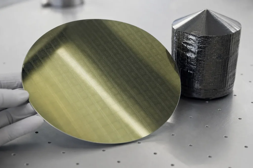
Silicon carbide (SiC) is a group IV-IV compound semiconductor of silicon and carbon with a wide, indirect bandgap of about 3.26 eV in its 4H polytype. A critical field about ten times silicon’s and roughly three times silicon’s thermal conductivity make 4H-SiC the leading material for 1,200 V power devices and EV inverters.
Key takeaways
- 4H-SiC: bandgap about 3.26 eV, critical field about 2.5 to 3 MV/cm, thermal conductivity about 330 to 490 W/m·K.
- SiC power devices are vertical and run from 650 V to 1,700 V in volume, with 3.3 kV parts available.
- Crystal growth is slow and defect-prone, which keeps SiC wafers far more expensive than silicon.
- Pick SiC over GaN at 1,200 V and above, and wherever heat removal and avalanche ruggedness matter.
Key numbers at 300 K
Values are for 4H-SiC, the polytype used in power devices, at 300 K, with silicon as the baseline. A polytype is one of the many stacking sequences SiC can crystallise in.
| Property (300 K) | 4H-SiC | Si (reference) |
|---|---|---|
| Crystal structure | Hexagonal (4H polytype) | Diamond cubic |
| Lattice constant (Å) | a = 3.073, c = 10.053 | 5.431 |
| Bandgap (eV) | 3.23 to 3.26, indirect | 1.12, indirect |
| Bandgap, other polytypes (eV) | 6H about 3.0; 3C about 2.36 | — |
| Electron mobility, bulk (cm²/V·s) | Up to about 900 to 1,000 | About 1,400 |
| Electron mobility, MOSFET channel (cm²/V·s) | Often well under 100 | Several hundred |
| Hole mobility (cm²/V·s) | Up to about 120 | About 450 |
| Critical field (MV/cm) | About 2.5 to 3 | About 0.3 |
| Saturation velocity (107 cm/s) | About 2.0 | About 1.0 |
| Thermal conductivity (W/m·K) | About 330 to 490 | About 150 |
| Static dielectric constant | About 9.7 | 11.7 |
| Density (g/cm³) | 3.21 | 2.33 |
What is silicon carbide?
SiC is a covalent network solid: every silicon atom is bonded to four carbon atoms in a tetrahedron, and the bonds run through the whole crystal. That structure makes it extremely hard, about 9 to 9.5 on the Mohs scale against diamond’s 10, and chemically inert. The same layers of tetrahedra can stack in many sequences, giving more than 200 known polytypes. The three that matter are 4H and 6H (hexagonal) and 3C (cubic).
Because it combines two group IV elements, SiC is a compound semiconductor, but not a III-V. Long before electronics, SiC was an abrasive and a structural ceramic. See SiC’s crystal structure, the main SiC polytypes and how SiC is classified.
Why is 4H-SiC used for power devices?
4H has the widest bandgap of the common polytypes and the most uniform electron mobility along the growth axis, which is the direction current flows in a vertical device. 6H has lower mobility along that axis; 3C has a smaller gap. 4H also has the most mature wafers and epitaxy.
The wide gap keeps the intrinsic carrier concentration, the thermally generated electrons, tiny even at several hundred degrees Celsius, so devices stay controllable where silicon would leak. Pure SiC is an insulator; it conducts only when doped with nitrogen or aluminium. See why SiC suits power electronics, SiC as a high-temperature semiconductor and whether SiC is electrically conductive.
What SiC devices exist?
The commercial line-up is Schottky barrier diodes (SBDs), MOSFETs, JFETs and power modules that combine them. Ratings run from 650 V to 1,700 V in volume, with 3.3 kV parts available. The main users are EV traction inverters, onboard chargers, solar inverters, industrial drives and rail traction. The known weakness is the gate oxide interface, which cuts MOSFET channel mobility well below bulk. See the SiC device portfolio and SiC’s loss and frequency gains over silicon.
EV traction is the volume driver. An 800 V battery pack needs switches rated about 1,200 V, a class where silicon IGBTs carry high switching and tail-current losses. SiC MOSFETs cut those losses, which shrinks the cooling system and stretches range from the same battery. The same logic applies to fast DC chargers and solar inverters, which also work at high voltage and run long duty cycles.
Beyond power, SiC serves UV photodiodes, MEMS for harsh environments and radiation detectors. Our guides cover optical devices, MEMS, radiation hardness and high-temperature sensors and electronics.
How is SiC made?
Abrasive-grade SiC comes from the Acheson process, which heats silica sand and carbon in an electric furnace. Electronic-grade crystals are grown by physical vapour transport (PVT): SiC powder sublimes above about 2,000 °C and recondenses on a seed crystal. Growth is slow, a fraction of a millimetre per hour, against far faster silicon pulling. Device layers are then grown by chemical vapour deposition. See how SiC is made.
Two defects dominate yield. Micropipes are hollow screw dislocations that kill devices outright. Basal plane dislocations (BPDs) can grow into stacking faults under forward current and raise on-resistance over time. Volume production is on 150 mm wafers, with 200 mm ramping. See SiC wafers, micropipes and BPDs and the industry outlook.
How does SiC compare with Si and GaN?
Against a silicon IGBT at 1,200 V, a SiC MOSFET switches faster with much lower switching loss, so converters run at higher frequency with smaller passives. Against GaN, SiC trades some switching speed for two to three times the thermal conductivity, avalanche ruggedness and a voltage range GaN does not yet reach commercially. The two overlap at 650 V. Against silicon the cost gap is the main brake: a SiC die still costs several times a silicon die of the same rating, so SiC wins where its lower losses pay back in cooling, size or battery capacity. Below about 600 V and at low frequency, silicon MOSFETs and IGBTs usually remain the cheaper answer. Side-by-side data is in our comparisons section, and the materials index places SiC among all other materials.
Start here
- Understanding Silicon Carbide and its Properties
- SiC Wafers: 150 mm vs 200 mm, Micropipes and Basal Plane Dislocations
- Silicon Carbide (SiC) Devices Revolutionizing Energy Efficiency and Performance
All silicon carbide guides
Properties and structure
- Understanding Silicon Carbide and its Properties
- Silicon Carbide (SiC): An Emerging Powerhouse in High-Power Semiconductor Applications
- What is SiC structure?
- Is SiC a network solid?
- Is silicon carbide stronger than diamond?
- Is SiC electrically conductive?
- Is silicon carbide a compound semiconductor?
- Understanding Silicon Carbide (SiC) as a Ceramic Material
Power devices
- Silicon Carbide (SiC) Devices Revolutionizing Energy Efficiency and Performance
- Understanding Silicon Carbide as a Semiconductor in Power Electronics
- Enhanced Performance of Silicon Carbide in Power Applications
High-temperature, optical, MEMS and radiation uses
- Turning Up the Heat: Unleashing Silicon Carbide’s Potential as a High-Temperature Semiconductor
- Silicon Carbide as a Material for High-Temperature Applications
- Silicon Carbide as a Material for Optical Devices
- Silicon Carbide as a Material for MEMS Devices
- Silicon Carbide as a Material for Radiation Hardness
Manufacturing, wafers and outlook
- How is SiC made?
- SiC Wafers: 150 mm vs 200 mm, Micropipes and Basal Plane Dislocations
- Future Prospects of Silicon Carbide in the Semiconductor Industry
Compound semiconductor background
- Understanding the Basics of Compound Semiconductors
- What is a Compound Semiconductor
- What Are III-V Semiconductors? Members, Properties and Uses
- What Is a Wide-Bandgap Semiconductor?
- Semiconductors Examples
General FAQs
- What materials are semiconductors?
- What are types of semiconductor?
- What are the advantages of compound semiconductors?
- What is a semiconductor made of?
- What are examples of compound semiconductors?
Related material hubs
Head-to-head comparisons
- GaN vs SiC: Properties, Voltage Range and Which to Choose
- SiC MOSFET vs Si IGBT: Losses, Switching Frequency and Cost
- SiC Wafers: 150 mm vs 200 mm, Micropipes and Basal Plane Dislocations
- Breakdown Field of Semiconductors Compared
SiC process deep dives
- SiC Epitaxy: CVD Step-Flow Growth on Off-Axis Wafers
- Doping Silicon Carbide: Nitrogen, Aluminium and Implant Activation
- SiC Gate Oxide: Interface Traps, Channel Mobility and Threshold Drift
FAQ
Is SiC a semiconductor or a ceramic?
Both. The same compound is sold as an abrasive and structural ceramic, and, as high-purity doped single crystals, as a wide-bandgap semiconductor.
Why are SiC wafers expensive?
Crystals grow by sublimation above about 2,000 °C at a fraction of a millimetre per hour, and defects such as micropipes and basal plane dislocations cut yield.
Can SiC devices run hotter than silicon?
Yes. The 3.26 eV gap keeps thermally generated carriers low at temperatures where silicon junctions leak heavily. In practice, packaging often sets the limit before the die does.
Sources
- Ioffe Institute, New Semiconductor Materials (NSM) archive, http://www.ioffe.ru/SVA/NSM/Semicond/
- T. Kimoto and J. A. Cooper, Fundamentals of Silicon Carbide Technology, Wiley-IEEE Press.
- B. J. Baliga, Fundamentals of Power Semiconductor Devices, Springer.
- S. M. Sze and K. K. Ng, Physics of Semiconductor Devices, 3rd ed., Wiley.
