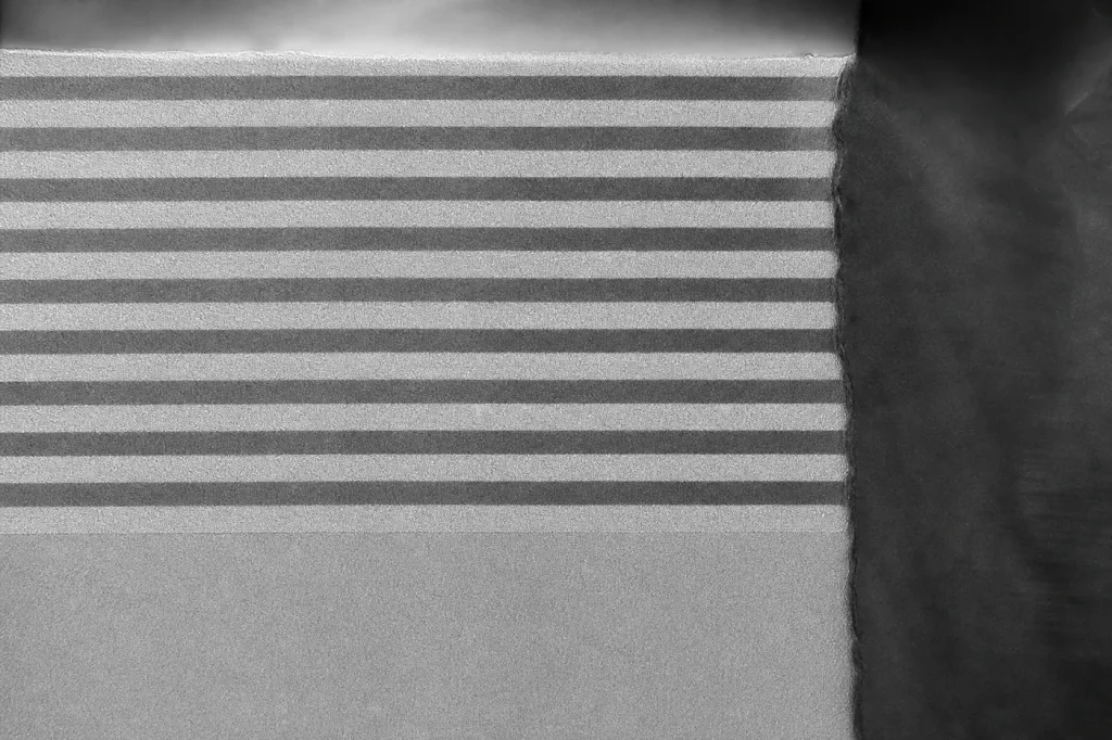
AlGaAs/GaAs heterostructures are stacks of AlxGa1−xAs and GaAs layers that combine different bandgaps with an almost identical lattice constant, mismatched by only about 0.14% even at x = 1. That near-perfect match lets engineers trap electrons and light in thin layers without strain. It is the basis of HEMTs, quantum-well lasers and VCSELs.
Key takeaways
- Lattice constants: GaAs 5.6533 Å, AlAs about 5.661 Å. The mismatch is about 0.14% for AlAs and scales roughly linearly with x.
- The bandgap rises from 1.424 eV (GaAs) at about 1.247 eV per unit x while the gap stays direct.
- The direct-to-indirect crossover sits near x ≈ 0.45, at a bandgap of about 1.98 eV.
- For x below 0.45, roughly 60% of the bandgap difference falls in the conduction band and 40% in the valence band.
- Modulation doping, reported by Dingle and colleagues in 1978, separates electrons from their donors and led directly to the HEMT.
What is a heterostructure?
A heterostructure is a crystal made of two or more different semiconductors grown on top of each other, with a sharp interface called a heterojunction. Because the materials have different bandgaps, the conduction and valence band edges step up or down at the interface. Those steps, the band offsets, can confine electrons, holes or both to one layer.
The hard part is growing one crystal on another without defects. If the two lattice constants differ, the top layer is strained. Beyond a critical thickness, the strain relaxes by forming misfit dislocations, which ruin electrical and optical quality. AlGaAs/GaAs avoids this problem almost entirely. That is why it became the first, and still the most studied, heterostructure system. For the broader principle of tuning bandgap with composition, see our guide to semiconductor alloys and bandgap engineering.
Why is AlGaAs lattice-matched to GaAs?
Aluminium and gallium atoms are almost the same size in the zinc blende lattice. Swapping one for the other barely changes the bond length. As a result, AlAs has a lattice constant of about 5.661 Å against 5.6533 Å for GaAs at 300 K, according to the Ioffe Institute NSM archive and Adachi’s 1985 review of GaAs, AlAs and AlGaAs parameters.
The mismatch, (aAlAs − aGaAs)/aGaAs, is about 0.14%. The ternary alloy follows Vegard’s law, a linear interpolation between the end points, so Al0.3Ga0.7As is mismatched by only about 0.04%. Thick layers of any composition grow on GaAs with negligible strain.
Compare that with other systems. InGaAs on GaAs mismatches by about 7% at full indium. AlGaN on GaN mismatches by up to about 2.4% at full aluminium. Those systems work, but layer thickness and composition are limited by strain.
AlGaAs properties by aluminium fraction
The direct (Γ-valley) bandgap at 300 K follows Eg ≈ 1.424 + 1.247x eV for x below about 0.45. Above that, the indirect X-valley is lower, with Eg ≈ 1.900 + 0.125x + 0.143x2 eV. Both expressions are given in the Ioffe NSM archive.
| Al fraction x | Bandgap (eV, 300 K) | Gap type | Emission wavelength (nm) | Mismatch to GaAs | Typical role |
|---|---|---|---|---|---|
| 0 (GaAs) | 1.424 | Direct | About 870 | 0 | Channel, active layer, substrate |
| 0.15 | About 1.61 | Direct | About 770 | About 0.02% | Active layer for shorter-wavelength lasers |
| 0.30 | About 1.80 | Direct | About 690 | About 0.04% | HEMT barrier, laser cladding |
| About 0.45 | About 1.98 | Crossover | n/a | About 0.06% | Direct-indirect transition |
| 0.70 | About 2.06 | Indirect | n/a | About 0.10% | Cladding, DBR layers |
| 1.0 (AlAs) | About 2.17 | Indirect | n/a | About 0.14% | DBR low-index layer; oxidation source |
Where is the direct-indirect crossover in AlGaAs?
At an aluminium fraction of about x ≈ 0.45, where the bandgap is about 1.98 eV. Published values cluster between about 0.4 and 0.45, depending on the measurement and the interpolation used. Below the crossover, the lowest conduction-band minimum is at the Γ point, the centre of the Brillouin zone, and the gap is direct. Above it, the X-valley minimum drops below Γ and the gap becomes indirect.
This sets a hard design rule. Light-emitting layers must stay below about x = 0.45, because indirect-gap material emits poorly. In practice, AlGaAs active regions stay well below that, and red emission much shorter than about 700 nm moves to AlGaInP instead. High-aluminium layers are used where emission is not needed: as cladding to confine light, as barriers, and in mirrors.
The crossover also affects band offsets. Above x ≈ 0.45 the conduction-band offset to GaAs no longer grows, because the lowest conduction state switches valleys. Barriers for electron confinement therefore get no deeper as x rises past the crossover.
How are the band offsets split?
For direct-gap compositions, the bandgap difference ΔEg divides roughly 60:40 between the conduction band (ΔEc) and the valence band (ΔEv). Early optical work by Dingle, Wiegmann and Henry in 1974 suggested about 85:15. Later measurements in the mid-1980s revised this to about 60:40 to 65:35, the values used in device design today.
For Al0.3Ga0.7As on GaAs, ΔEg is about 0.37 eV, so ΔEc is roughly 0.22 to 0.24 eV and ΔEv roughly 0.13 to 0.15 eV. The alignment is type I: GaAs sits inside AlGaAs in energy, so both electrons and holes are confined in the GaAs layer. That is the arrangement a quantum-well laser needs. For band-diagram basics, see our energy bands section.
What is modulation doping?
Modulation doping puts the dopant atoms in one layer and lets the electrons they release collect in a neighbouring, undoped layer. R. Dingle, H. L. Störmer, A. C. Gossard and W. Wiegmann reported it in Applied Physics Letters in 1978, in work at Bell Labs on electron mobilities in modulation-doped AlGaAs/GaAs heterojunction superlattices.
The mechanism is straightforward. Silicon donors are placed in the AlGaAs barrier. The electrons they release fall across the interface into the lower-energy GaAs conduction band and pile up in a thin sheet at the interface. That sheet is a two-dimensional electron gas (2DEG). The ionised donors stay behind in the AlGaAs. An undoped AlGaAs spacer, typically a few nanometres to a few tens of nanometres thick, pushes them further away.
The payoff is mobility. In ordinary doped GaAs, electrons scatter off the ionised donors they came from. In a modulation-doped structure, they travel in pure GaAs, away from those donors. Room-temperature 2DEG mobility reaches about 7,000 to 8,000 cm²/V·s, close to the bulk lattice limit. At low temperature, where phonon scattering freezes out, the best structures have exceeded 107 cm²/V·s. Those samples underpinned the discovery of the fractional quantum Hall effect.
One complication is the DX centre. Silicon in AlGaAs with x above about 0.2 forms a deep donor state that traps electrons and causes persistent photoconductivity and threshold shifts. HEMT designers handle it by keeping x near 0.2 to 0.3, using delta doping, or moving to pseudomorphic structures.
What devices use AlGaAs/GaAs?
- HEMTs. Takashi Mimura and colleagues at Fujitsu reported the high-electron-mobility transistor in 1980, built on the modulation-doped AlGaAs/GaAs 2DEG. Production devices today are mostly pseudomorphic HEMTs (pHEMTs), which add a strained InGaAs channel for higher sheet charge and velocity. They serve LNAs, switches and mmWave front ends.
- HBTs. AlGaAs emitters on GaAs bases form heterojunction bipolar transistors. Commercial handset power amplifiers moved largely to InGaP emitters, which avoid DX-centre and oxidation issues, but the principle is the same.
- Lasers. The double-heterostructure laser, with a GaAs active layer between AlGaAs claddings, made room-temperature continuous-wave lasing practical around 1970. Quantum-well AlGaAs lasers near 780 nm to 850 nm followed for optical storage, printing and pumping.
- VCSELs. Vertical-cavity lasers use distributed Bragg reflectors (DBRs) made of alternating high- and low-aluminium layers. Lattice matching allows dozens of mirror pairs without strain. A high-aluminium layer, near AlAs, is wet-oxidised from the side to form a current-confining aperture.
- Research structures. Quantum wells, superlattices, quantum dots and quantum-well infrared photodetectors all grew up in this system.
High-aluminium AlGaAs has one practical drawback: it oxidises in air and moisture. Exposed layers are capped or passivated. For GaAs itself, see the GaAs materials hub and our page on the properties of gallium arsenide. For how AlGaAs/GaAs compares with nitride heterostructures, see the comparisons hub.
FAQ
How does an AlGaAs/GaAs 2DEG differ from an AlGaN/GaN 2DEG?
The AlGaAs/GaAs 2DEG comes from modulation doping. The AlGaN/GaN 2DEG forms mainly from spontaneous and piezoelectric polarisation, with no intentional barrier doping. GaN gives higher sheet density; GaAs gives higher mobility.
What aluminium fraction is used in HEMT barriers?
Usually about 0.2 to 0.3. That gives a conduction-band offset near 0.2 eV while limiting DX-centre effects from silicon doping.
Is AlAs a direct or indirect semiconductor?
Indirect, with a gap of about 2.17 eV at 300 K. AlGaAs turns indirect at x ≈ 0.45.
Why are VCSEL mirrors made from AlGaAs?
GaAs and AlAs differ in refractive index by roughly 0.5 near 850 nm while sharing the same lattice. Many strain-free layer pairs give reflectivity above 99%.
Sources
- R. Dingle, H. L. Störmer, A. C. Gossard and W. Wiegmann, “Electron mobilities in modulation-doped semiconductor heterojunction superlattices,” Applied Physics Letters (1978).
- T. Mimura, S. Hiyamizu, T. Fujii and K. Nanbu, paper on a new field-effect transistor with selectively doped GaAs/n-AlGaAs heterojunctions, Japanese Journal of Applied Physics (1980).
- S. Adachi, “GaAs, AlAs, and AlxGa1−xAs: Material parameters for use in research and device applications,” Journal of Applied Physics (1985).
- Ioffe Institute, New Semiconductor Materials (NSM) archive, aluminium gallium arsenide: band structure and basic parameters.
- S. M. Sze and K. K. Ng, Physics of Semiconductor Devices, 3rd ed., Wiley.



