How to choose a semiconductor material: start from the one property your application cannot compromise on. For power, that is blocking voltage and critical field. For RF, it is frequency and output power. For optics, it is wavelength, which the bandgap fixes. Then check whether silicon already meets it, and whether the substrate is affordable at volume.
Key takeaways
- Every application has one deciding property. Find it first and most of the field drops away.
- High-voltage power: SiC from 650 V to 3.3 kV, GaN at 650 V and below, Si IGBTs where frequency is low and cost dominates.
- RF: GaAs for handset power amplifiers, GaN for high-power infrastructure and radar, InP and SiGe for the highest frequencies.
- Optics: emission wavelength in µm is about 1.24 divided by bandgap in eV. 1550 nm needs InGaAsP or InGaAs on InP.
- Silicon wins whenever it is good enough, because it has 300 mm wafers and the deepest supply chain.
The method in five steps
- Name the hard constraint. A voltage, a frequency, a wavelength or a temperature. Write it down with units.
- Map it to a material property. Voltage maps to critical field. Frequency maps to saturation velocity and mobility. Wavelength maps to bandgap. Heat maps to thermal conductivity.
- Shortlist by that property. Use a property table and, for power, a figure of merit such as Baliga’s.
- Test silicon. If a silicon device meets the constraint with acceptable efficiency, it usually wins on cost and supply.
- Check the substrate. Wafer diameter, defect density and the number of qualified suppliers decide whether a material can ship at your volume.
Decision table: application, material, deciding property
The table covers the most common decisions. Material properties are 300 K values from the Ioffe Institute NSM archive and Sze and Ng. Voltage and frequency ranges describe general commercial status as of 2025, not any single product line.
| Application | Usual material | Deciding property | Typical range |
|---|---|---|---|
| Low-voltage power (below about 100 V) | Si MOSFET; GaN HEMT for high frequency | Channel resistance, gate charge | Si dominant; GaN for 48 V and high-density DC-DC |
| Power at 650 V | GaN HEMT, SiC MOSFET, Si superjunction | Switching loss vs ruggedness | All three compete |
| Power at 1,200 V to 3.3 kV | 4H-SiC MOSFET; Si IGBT at low frequency | Critical field (about 2.5 to 3 MV/cm for SiC vs 0.3 for Si) | SiC mainstream at 1,200 V and 1,700 V |
| Very high voltage (above about 3.3 kV) | Si IGBT, Si thyristor; SiC emerging | Bipolar conduction, cost | Si IGBT modules to several kV |
| Handset RF power amplifier | GaAs HBT (InGaP/GaAs) | Efficiency and linearity at 3 to 5 V battery voltage | Sub-6 GHz cellular bands |
| Base station and radar RF power | GaN-on-SiC HEMT; Si LDMOS below about 3 GHz | Power density (W/mm), thermal conductivity | L-band through Ka-band |
| mmWave and sub-THz transistors | InP HEMT and HBT, SiGe HBT, GaAs pHEMT | Electron velocity and mobility | InP above 100 GHz; SiGe for integrated radar and transceivers |
| Blue, green and white LEDs | InGaN/GaN | Direct bandgap, 3.39 eV for GaN | About 400 to 530 nm |
| Red and amber LEDs | AlGaInP on GaAs | Direct bandgap near 1.9 to 2.2 eV | About 570 to 650 nm |
| 850 nm VCSELs and lasers | GaAs/AlGaAs | Bandgap 1.42 eV (GaAs), lattice-matched mirrors | About 780 to 980 nm with InGaAs wells |
| 1310 and 1550 nm lasers | InGaAsP or InGaAlAs on InP | Bandgap tunable to about 0.8 eV, lattice-matched to InP | About 1.3 to 1.6 µm |
| Photodetectors, visible to 1.1 µm | Si | Bandgap 1.12 eV | Cutoff about 1.1 µm |
| Photodetectors, 1.0 to 1.7 µm | In0.53Ga0.47As on InP, Ge | Bandgap about 0.75 eV (InGaAs), 0.66 eV (Ge) | Cutoff about 1.65 µm for InGaAs |
Which semiconductor should I use for high voltage?
Above about 900 V, use 4H-SiC for fast switching and silicon IGBTs where switching frequency is low and cost matters most. The reason is critical field: the field a material holds before avalanche breakdown. 4H-SiC holds about 2.5 to 3 MV/cm, roughly ten times silicon’s 0.3 MV/cm. That lets a SiC drift layer be about ten times thinner and much more heavily doped for the same voltage, which cuts on-resistance by orders of magnitude. The Baliga figure of merit captures this in one number.
GaN has a similar critical field, about 3.3 MV/cm, but most commercial GaN power devices are lateral HEMTs on silicon. Their ratings cluster at 100 V to 650 V. At 650 V, GaN, SiC and silicon superjunction MOSFETs all compete. See GaN vs SiC for that head-to-head and SiC MOSFET vs Si IGBT for the 1,200 V decision.
Which semiconductor for RF above 10 GHz?
It depends on whether you need power or speed.
- For power above 10 GHz, use GaN-on-SiC. GaN HEMTs combine a critical field near 3.3 MV/cm with a saturation velocity near 2.5 × 107 cm/s. They run at 20 V to 50 V drain bias and deliver several watts per millimetre of gate width. The SiC substrate, at about 330 to 490 W/m·K, removes the heat. X-band radar and Ka-band satellite amplifiers use it.
- For low noise and moderate power, use GaAs pHEMT. A pseudomorphic HEMT (pHEMT) uses a strained InGaAs channel on GaAs for high electron mobility. It is mature, cheaper per wafer than GaN-on-SiC and widely used in LNAs and mmWave front ends.
- For the highest frequencies, use InP or SiGe. InP HEMTs and HBTs have demonstrated cutoff frequencies well above 500 GHz in research. SiGe HBTs sit in silicon BiCMOS processes, so they win where a radar or transceiver needs digital logic on the same chip, such as 77 GHz automotive radar.
Our GaN vs GaAs for RF page covers power density and linearity in detail.
Which semiconductor for lasers at 1550 nm?
Use InGaAsP or InGaAlAs quantum wells grown on InP. Wavelength follows bandgap: λ (µm) ≈ 1.24 / Eg (eV). 1550 nm needs a bandgap of about 0.80 eV. GaAs, at 1.42 eV, emits near 870 nm and cannot reach it while staying lattice-matched. InP, at 1.34 eV, is the substrate; quaternary alloys lattice-matched to it can be tuned from about 0.75 eV to 1.34 eV. That covers the 1310 nm and 1550 nm fibre windows.
Silicon cannot emit efficiently because its bandgap is indirect. Silicon photonics uses silicon for waveguides and modulators, with InP-based lasers bonded or attached. Germanium on silicon serves as the detector.
When is silicon good enough?
More often than marketing suggests. Silicon is the default when:
- The power device runs below about 100 V and the switching frequency is moderate. Silicon trench MOSFETs are cheap and very low resistance.
- The power device switches slowly at high voltage, such as a line-frequency or low-kHz motor drive. Silicon IGBTs handle this well.
- The RF front end needs digital integration and modest output power. CMOS and SiGe BiCMOS dominate Wi-Fi and Bluetooth radios.
- The detector works between visible light and about 1.1 µm, set by silicon’s 1.12 eV bandgap. Camera sensors are silicon.
Silicon stops being good enough when the hard constraint falls on a property it simply lacks: a critical field above 0.3 MV/cm, a direct bandgap, or emission outside its range. In fast-switching power conversion, that line usually falls somewhere between 100 V and 650 V.
How much does substrate cost matter?
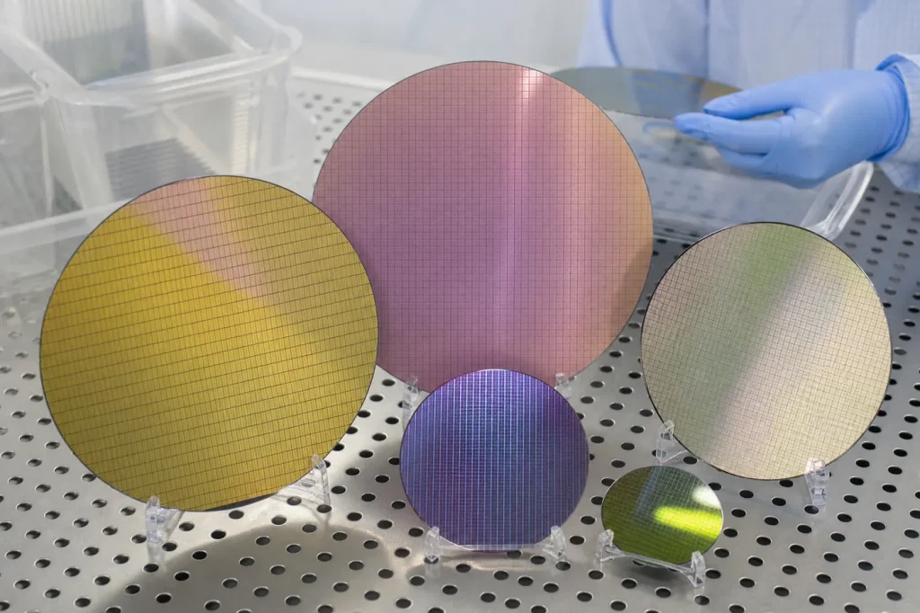
A great deal, though we do not quote prices here because they change quickly and vary by contract. The structural facts are stable. Wafer diameter sets how many die each run produces, and larger fabs need larger wafers. As of 2025, general supplier status looks like this:
| Material | Typical production wafer diameter | Availability note |
|---|---|---|
| Si | 300 mm (200 mm for power and analog) | Deepest supply chain |
| GaAs | 150 mm for RF; 100 mm and smaller common in optoelectronics | Mature, several suppliers |
| 4H-SiC | 150 mm in volume, 200 mm ramping | Substrate is a large share of device cost |
| GaN | Native wafers small and costly; GaN usually grown on Si (150 to 200 mm) or SiC | Substrate choice sets cost and thermal path |
| InP | Typically 75 mm to 100 mm; 150 mm emerging | Smaller volume, higher cost per area |
The practical rule: a compound semiconductor has to earn its substrate. GaN-on-Si exists because it moves GaN onto cheaper, larger silicon wafers. SiC’s move from 150 mm to 200 mm matters for the same reason. For the full property data behind this guide, use our semiconductor properties table and the comparisons hub.
FAQ
What is the single most important property when choosing a semiconductor?
There is no single one. Bandgap is the most common deciding property because it drives critical field, emission wavelength and maximum operating temperature together. But the application decides which consequence of bandgap matters.
Why not use the widest bandgap material for everything?
Wider bandgap materials usually have smaller, costlier substrates, harder doping (especially p-type) and less mature processing. They only pay off when the application needs what the wide bandgap provides.
How do I convert bandgap to wavelength?
Divide 1.24 by the bandgap in eV to get the wavelength in µm. GaAs at 1.42 eV gives about 0.87 µm; GaN at 3.39 eV gives about 0.37 µm.
Is GaAs still used now that GaN exists?
Yes. GaAs HBTs remain the standard for handset power amplifiers, and GaAs/AlGaAs is the platform for 850 nm VCSELs and red LEDs. GaN replaced other technologies mainly in high-power RF.
Sources
- S. M. Sze and K. K. Ng, Physics of Semiconductor Devices, 3rd ed., Wiley.
- B. J. Baliga, Fundamentals of Power Semiconductor Devices, Springer.
- Ioffe Institute, New Semiconductor Materials (NSM) archive, characteristics and properties of Si, Ge, GaAs, InP, GaN, SiC and their alloys.
- U. K. Mishra, P. Parikh and Y.-F. Wu, “AlGaN/GaN HEMTs: an overview of device operation and applications,” Proceedings of the IEEE (2002).
- T. Kimoto and J. A. Cooper, Fundamentals of Silicon Carbide Technology, Wiley-IEEE Press.