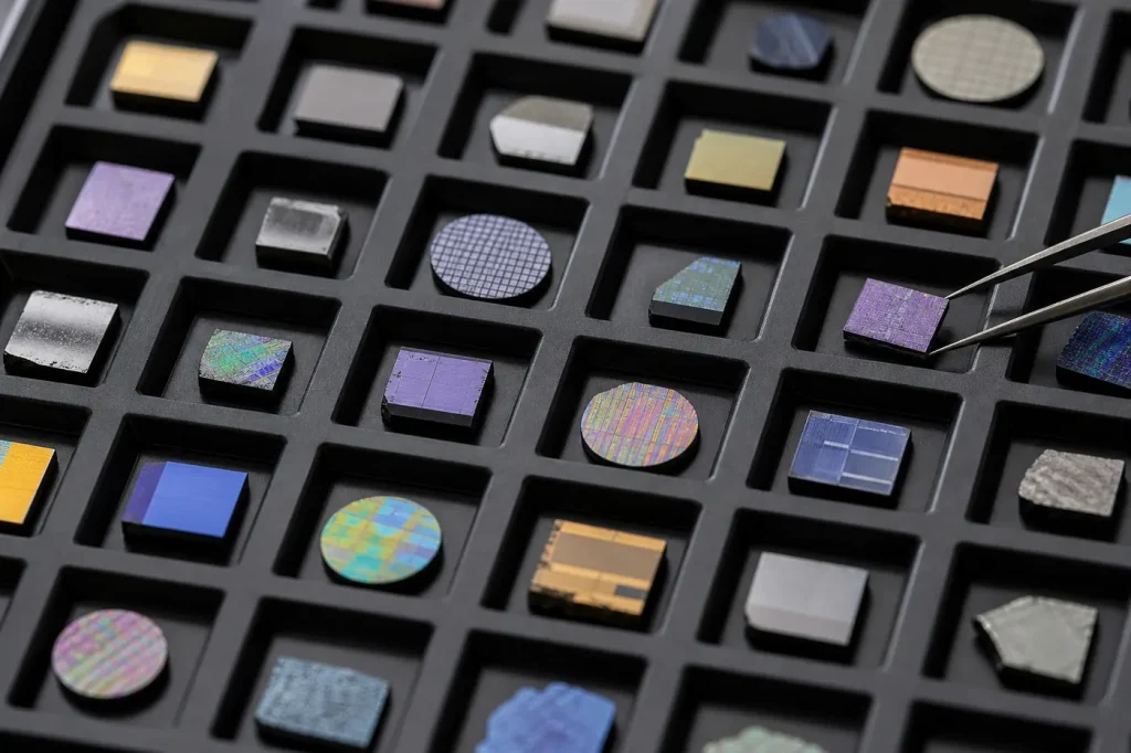
A semiconductor properties table is a side-by-side reference of the core electronic, thermal and structural constants of semiconductor materials at a stated temperature. This one covers 20 materials at 300 K, from InSb (0.17 eV bandgap) to AlN (about 6.2 eV), compiled from the Ioffe Institute NSM archive and standard references.
Key takeaways
- All values are at 300 K for undoped or lightly doped material. Mobilities are upper limits; doping, defects and alloy scattering lower them.
- InSb has the highest electron mobility, up to about 77,000 cm²/V·s. Diamond has the highest thermal conductivity, about 2,000–2,200 W/m·K, and one of the highest critical fields, about 10 MV/cm.
- The GaAs lattice constant is 5.653 Å, almost identical to AlAs (5.661 Å), which is why AlGaAs grows lattice-matched on GaAs.
- Critical field and thermal conductivity are the most disputed columns. Where sources disagree we give a range; where we are not confident we leave the cell as “—”.
The table: 20 semiconductors at 300 K
Column key: Eg is bandgap in eV; D means a direct gap and I an indirect gap. μn and μp are electron and hole mobility in cm²/V·s. Ec is critical (breakdown) field in MV/cm. κ is thermal conductivity in W/m·K. εr is the static relative permittivity. a is the lattice constant in Å; for hexagonal crystals both a and c are given.
| Material | Structure | Eg (eV) | Gap | μn (cm²/V·s) | μp (cm²/V·s) | Ec (MV/cm) | κ (W/m·K) | εr | Lattice constant (Å) |
|---|---|---|---|---|---|---|---|---|---|
| Si | Diamond cubic | 1.12 | I | ≤1,400 | ≤450 | ~0.3 | 130–150 | 11.7 | 5.431 |
| Ge | Diamond cubic | 0.66 | I | ≤3,900 | ≤1,900 | ~0.1 | 58 | 16.2 | 5.658 |
| GaAs | Zinc blende | 1.42 | D | ≤8,500 | ≤400 | ~0.4 | 55 | 12.9 | 5.653 |
| InP | Zinc blende | 1.34 | D | ≤5,400 | ≤200 | ~0.5 | 68 | 12.5 | 5.869 |
| GaP | Zinc blende | 2.26 | I | ≤250 | ≤150 | ~1 | 110 | 11.1 | 5.451 |
| InAs | Zinc blende | 0.354 | D | ≤40,000 | ≤500 | ~0.04 | 27 | 15.2 | 6.058 |
| InSb | Zinc blende | 0.17 | D | ≤77,000 | ≤850 | ~0.001 | 18 | 16.8 | 6.479 |
| GaSb | Zinc blende | 0.726 | D | ≤3,000 | ≤1,000 | ~0.05 | 32 | 15.7 | 6.096 |
| AlAs | Zinc blende | 2.12–2.16 | I | — | — | — | 91 | 10.1 | 5.661 |
| In0.53Ga0.47As | Zinc blende (alloy) | 0.75 | D | ≤12,000 | ≤300 | — | ~5 | 13.9 | 5.869 (matched to InP) |
| GaN | Wurtzite | 3.39 | D | ≤1,000 (bulk); ~2,000 (2DEG) | ≤200 | ~3.3 | 130–230 | 8.9 | a 3.189, c 5.185 |
| AlN | Wurtzite | ~6.2 | D | ~300 | — | ~12 (estimated) | 285–320 | 8.5 | a 3.112, c 4.982 |
| InN | Wurtzite | ~0.7 | D | — | — | — | — | 15.3 | a 3.545, c 5.703 |
| 4H-SiC | Hexagonal | 3.26 | I | ≤900 | ≤120 | ~2–3 | ~370 | 9.7 | a 3.073, c 10.053 |
| 6H-SiC | Hexagonal | ~3.0 | I | ≤400 | ≤90 | ~2.5–3 | ~490 | 9.7 | a 3.081, c 15.12 |
| 3C-SiC | Zinc blende | 2.36 | I | ≤1,000 | ≤40 | ~1 | ~360 | 9.7 | 4.360 |
| Diamond (C) | Diamond cubic | 5.47 | I | ≤2,200 | ≤1,800 | ~10 | 2,000–2,200 | 5.7 | 3.567 |
| β-Ga2O3 | Monoclinic | ~4.8 | I (nearly direct) | ~150–200 | — | ~8 (estimated) | ~10–27 (direction-dependent) | ~10 | a 12.2, b 3.04, c 5.80 |
| ZnO | Wurtzite | 3.37 | D | ~200 | — | — | — | ~8.7 | a 3.250, c 5.207 |
| CdTe | Zinc blende | ~1.5 | D | ~1,000 | ~100 | — | ~6 | ~10.4 | 6.481 |
Each column has its own deep-dive: bandgap in Decoding the Bandgap, mobility in our charge carrier mobility guide, thermal conductivity in Semiconductors and Heat, dielectric constant in our dielectric constant comparison and critical field in our breakdown field comparison.
How to read the table
Bandgap and gap type
The bandgap is the energy needed to lift an electron from the valence band into the conduction band. In a direct-gap material, the lowest conduction-band state sits directly above the highest valence-band state in momentum, so electrons and holes recombine efficiently by emitting light. That is why LEDs and lasers use GaAs, InP, GaN and their alloys, while silicon, an indirect-gap material, does not emit light well. Bandgap shrinks as temperature rises, so a 300 K value will not match a 77 K or 4 K measurement.
Mobility
Mobility is how fast a carrier drifts per unit electric field. The Ioffe archive gives most values as upper limits for pure crystals, which is why many cells start with “≤”. Real devices see lower values once dopants, interfaces and defects scatter the carriers. GaN is the important exception in the other direction: the two-dimensional electron gas at an AlGaN/GaN interface reaches about 2,000 cm²/V·s, higher than bulk GaN. Our GaN properties table covers that in detail.
Critical field
The critical field is the electric field at which avalanche breakdown sets in. It rises steeply with bandgap and also depends on doping, so it is the softest column in the table. Wide-bandgap values for GaN, AlN and Ga2O3 started as theoretical estimates.
Thermal conductivity, permittivity and lattice constant
Thermal conductivity sets how easily a device sheds heat. It falls with rising temperature, with impurities and with dislocations, and it collapses in alloys: In0.53Ga0.47As conducts heat about 5 to 11 times worse than InAs or GaAs. Permittivity sets capacitance and enters power-device figures of merit. The lattice constant decides which materials can be grown on which substrates without strain; mismatched layers relax by forming dislocations.
Which semiconductor has the highest electron mobility?
InSb, at up to about 77,000 cm²/V·s at 300 K, followed by InAs at up to about 40,000 cm²/V·s. Both have very small bandgaps (0.17 eV and 0.354 eV) and very light electron effective masses. The trade-off is clear in the same rows: their critical fields are tiny and they conduct heavily at room temperature, so they suit infrared detectors, Hall sensors and very-high-speed low-voltage transistors, not power devices. Among materials that are practical for transistors at room temperature, GaAs (up to about 8,500 cm²/V·s) and In0.53Ga0.47As (up to about 12,000 cm²/V·s) lead. For more on the III-V family, see our III-V semiconductors guide.
What is the lattice constant of GaAs?
GaAs has a zinc-blende lattice constant of 5.653 Å at 300 K. AlAs is 5.661 Å, a mismatch of only about 0.15%, so AlxGa1−xAs layers of any composition grow on GaAs with little strain. Germanium (5.658 Å) is also close, which is why GaAs solar cells for space are grown on Ge substrates. InP (5.869 Å) is the other common III-V substrate, and In0.53Ga0.47As is the composition that matches it.
Which values are disputed?
- InN bandgap. Older literature gave about 1.9 eV. Better crystals grown in the early 2000s showed a gap of about 0.7 eV, and the older figure is now attributed to impurities and oxygen. Some older tables still carry the high value.
- GaN thermal conductivity. The Ioffe archive lists 130 W/m·K. Low-dislocation bulk GaN measures substantially higher, around 200–230 W/m·K. Thin GaN-on-Si or GaN-on-sapphire layers measure lower.
- Silicon thermal conductivity. Ioffe gives 130 W/m·K; many handbooks give about 148–150 W/m·K. The difference reflects sample purity and measurement method.
- 4H-SiC critical field. The Ioffe archive gives 3–5 MV/cm. Device designers usually work with about 2–3 MV/cm at drift-layer doping.
- Ga2O3 and AlN critical fields. Both are estimates; measured device fields so far are lower.
- Diamond mobility. Ioffe lists up to 2,200 and 1,800 cm²/V·s for electrons and holes. Some later measurements on very pure single-crystal diamond reported higher values, but results vary with sample quality.
- β-Ga2O3 gap type. It is usually described as indirect, with a direct transition only slightly higher in energy, so it absorbs almost like a direct-gap material.
Measurement caveats
- Temperature. Every value here is at 300 K. Mobility and thermal conductivity both fall as temperature rises, often steeply.
- Anisotropy. Hexagonal and monoclinic crystals (GaN, AlN, InN, ZnO, SiC, Ga2O3) have direction-dependent mobility, permittivity and thermal conductivity. We give the commonly quoted value or a range.
- Doping. Mobilities are for pure or lightly doped material. Critical field rises with doping.
- Thin films vs bulk. Epitaxial layers on foreign substrates usually have more defects and lower mobility and thermal conductivity than bulk crystals.
Quick comparisons from the table
| Question | Leader in this table | Value (300 K) |
|---|---|---|
| Widest bandgap | AlN | ~6.2 eV |
| Narrowest bandgap | InSb | 0.17 eV |
| Highest electron mobility | InSb | ≤77,000 cm²/V·s |
| Highest hole mobility | Ge | ≤1,900 cm²/V·s |
| Highest thermal conductivity | Diamond | 2,000–2,200 W/m·K |
| Highest critical field (practical device material) | Diamond | ~10 MV/cm |
| Lowest permittivity | Diamond | 5.7 |
For power electronics, the row-by-row comparisons that matter most are Si, 4H-SiC and GaN. See our GaN vs silicon guide and GaN vs SiC for those trade-offs.
Frequently asked questions
Where do these values come from?
Most rows follow the Ioffe Institute NSM archive, the most widely used free reference for semiconductor constants. Materials it does not cover, such as β-Ga2O3, ZnO and CdTe, use standard handbooks and review literature.
Why are some cells marked “—”?
Because we could not confirm a reliable, widely agreed value. Hole mobility in Ga2O3, AlN and ZnO, for example, is very low and hard to measure because p-type doping is difficult or impossible. We prefer a blank cell to a guess.
What does the “≤” sign mean in the mobility columns?
It marks the upper limit for pure, undoped crystal at 300 K, as listed in the Ioffe archive. Doped or defective material has lower mobility.
Which semiconductor is best for power devices?
For production devices today, 4H-SiC and GaN. They combine a critical field roughly 7 to 11 times silicon’s with mature substrates and doping. Diamond and Ga2O3 have higher fields but are still research-stage for most power uses.
Sources
- Ioffe Institute, New Semiconductor Materials (NSM) archive: individual material pages. http://www.ioffe.ru/SVA/NSM/Semicond/
- O. Madelung, Semiconductors: Data Handbook, 3rd ed., Springer.
- S. M. Sze and K. K. Ng, Physics of Semiconductor Devices, 3rd ed., Wiley (appendix property tables).
- T. Kimoto and J. A. Cooper, Fundamentals of Silicon Carbide Technology, Wiley-IEEE Press (SiC polytype properties).
- Review literature on β-Ga2O3 materials and devices, and on the revised InN bandgap.



