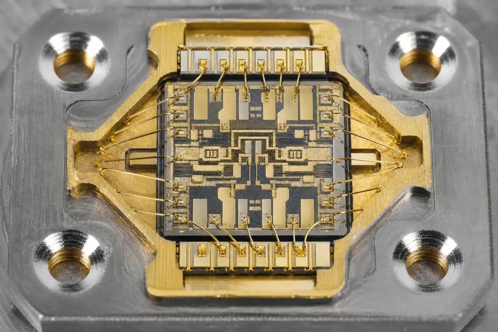
GaN vs GaAs for RF: GaN leads on power density (about 5 to 10 W/mm against roughly 1 W/mm for GaAs), breakdown voltage and heat handling. GaAs leads on low-voltage efficiency, noise, maturity and cost per wafer. Pick GaN for base stations, radar and satellite amplifiers. Pick GaAs for handset power amplifiers and low-noise front ends.
Key takeaways
- Bandgap 3.39 eV for GaN vs 1.42 eV for GaAs. Critical field is about eight times higher in GaN (about 3.3 vs 0.4 MV/cm).
- GaAs has far higher bulk electron mobility (about 8,500 vs about 1,000 cm²/V·s), but GaN has higher saturation velocity (about 2.5 vs about 1 × 107 cm/s).
- GaN HEMTs run at 28 V to 50 V drain bias; GaAs devices typically run at 3 V to 12 V. Higher voltage is the main source of GaN’s power density.
- GaN-on-SiC sits on a substrate that conducts heat at about 330 to 490 W/m·K, against about 55 W/m·K for GaAs.
- As of 2025, GaAs HBTs still dominate handset PAs; GaN-on-SiC dominates new high-power infrastructure and defence amplifiers.
GaN vs GaAs: material properties side by side
Values are for wurtzite GaN and zinc blende GaAs at 300 K. Device-channel values are given separately because RF transistors in both materials conduct through a two-dimensional electron gas (2DEG), a thin sheet of electrons at a heterojunction.
| Property (300 K) | GaN | GaAs | Edge |
|---|---|---|---|
| Bandgap (eV) | 3.39, direct | 1.424, direct | GaN |
| Critical field (MV/cm) | About 3.3 | About 0.4 | GaN |
| Electron mobility, bulk (cm²/V·s) | Up to about 1,000 | Up to about 8,500 | GaAs |
| Electron mobility, 2DEG channel (cm²/V·s) | About 1,500 to 2,000 (AlGaN/GaN) | About 6,000 to 8,000 (AlGaAs/GaAs, InGaAs pHEMT) | GaAs |
| 2DEG sheet density (cm−2) | About 1 × 10¹³ | About 1 to 3 × 10¹² | GaN |
| Saturation velocity (107 cm/s) | About 2.5 | About 1 (peak about 2) | GaN |
| Thermal conductivity (W/m·K) | About 130 to 230 | About 55 | GaN |
| Typical substrate | SiC (about 330 to 490 W/m·K) or Si | Semi-insulating GaAs | GaN on SiC |
| Static dielectric constant | About 8.9 | 12.9 | Context dependent |
The table explains the split. GaAs electrons move faster at low fields, which helps gain and noise at low voltage. GaN holds about eight times the field, carries about five times the sheet charge and keeps electrons faster once they saturate. Multiply voltage by current and GaN wins on power. Johnson’s figure of merit, the product of critical field and saturation velocity, puts GaN at roughly 20 times GaAs. Our article on Baliga and Johnson figures of merit shows the calculation.
How does power density compare?
Power density is RF output power per millimetre of gate width, in W/mm. It sets how large a transistor must be for a given output, and so its capacitance, matching difficulty and cost.
- GaAs pHEMTs and HBTs typically deliver well under 1 W/mm to about 1 W/mm. They are limited by low breakdown voltage, which caps drain voltage at a few to about 12 V.
- GaN HEMTs in production designs commonly run at about 5 to 10 W/mm at 28 V to 50 V. Mishra, Parikh and Wu’s 2002 review placed GaN roughly an order of magnitude above GaAs on this measure.
- Research records are higher. Y.-F. Wu and colleagues reported more than 30 W/mm from field-plated GaN HEMTs on SiC in IEEE Electron Device Letters in 2004. Records like this are not sustainable in products, where thermal limits and reliability set the operating point.
Ten times the power density means a GaN die roughly one-tenth the gate width for the same output. Smaller die have lower capacitance per watt, and higher drain voltage means higher output impedance, closer to 50 Ω. Both make wideband matching easier. That is a large part of why GaN suits wideband radar and electronic warfare.
Heat is the catch. Ten times the power in one-tenth the area concentrates heat. GaN-on-SiC handles it because SiC spreads heat six to nine times better than GaAs. GaN-on-Si is cheaper but closer to silicon’s 130 to 150 W/m·K. See GaN-on-Si vs GaN-on-SiC for that trade.
Why is GaN replacing GaAs in base stations?
Strictly, GaN in macro base stations mostly replaced silicon LDMOS, not GaAs. LDMOS (laterally diffused MOS) was the incumbent for high-power cellular PAs below about 3 GHz. GaAs served lower-power roles: driver stages, small cells and some medium-power amplifiers.
Three changes favoured GaN over both. First, cellular bands moved higher, to 3.3 GHz to 4.2 GHz and above for 5G, where LDMOS efficiency drops. Second, wider signal bandwidths rewarded GaN’s easier wideband matching. Third, massive MIMO radios pack many PAs into a small, passively cooled enclosure, so efficiency and heat handling per watt matter more than ever. GaN-on-SiC in Doherty amplifier configurations became the standard answer. As of 2025, that is the general industry status for new sub-6 GHz macro radios; LDMOS remains in lower bands.
Which is better for handset PAs?
GaAs, and by a clear margin today. Handset PAs run from a single lithium-ion cell, nominally about 3.7 V, with peak output of only a few watts or less. GaN’s main advantage, high-voltage operation, is wasted at that supply. GaAs HBTs with InGaP emitters deliver high efficiency and good linearity at that voltage. They also integrate well with GaAs pHEMT switches in front-end modules and come from a mature, high-volume 150 mm supply chain. As of 2025, InGaP/GaAs HBTs remain the dominant handset PA technology, with CMOS and SOI used in some lower-tier and integrated designs.
GaN for handsets is under active development, mostly GaN-on-Si for mmWave and higher-voltage supply schemes. It is not the mainstream choice. For more on GaAs in microwave circuits, see GaAs in microwave semiconductor devices.
How do efficiency and linearity compare?
Efficiency here means power-added efficiency (PAE): RF power added divided by DC power drawn. Linearity means how faithfully the amplifier reproduces a complex signal without spreading energy into adjacent channels.
- At high power, GaN is more efficient. Higher voltage swing and lower parasitics per watt suit high-efficiency classes and Doherty architectures at tens to hundreds of watts.
- At low voltage and low power, GaAs is efficient and well understood. Its linearity behaviour is mature and well modelled, which simplifies handset design.
- GaN has trapping effects. Charge trapping in the buffer and at the surface causes current collapse and memory effects. Base stations correct this with digital predistortion (DPD), which pre-shapes the signal to cancel amplifier distortion.
- Noise. GaAs pHEMTs offer very low noise figures and remain standard in LNAs. GaN LNAs are slightly noisier but survive large input signals without a limiter, which suits radar receivers.
Cost, frequency and maturity
| Factor | GaN (mainly on SiC) | GaAs |
|---|---|---|
| Typical drain or collector voltage | 28 V to 50 V | About 3 V to 12 V |
| Production power density | About 5 to 10 W/mm | Roughly 1 W/mm or less |
| Production frequency range | L-band through Ka-band; W-band in research | Sub-GHz through mmWave with short-gate pHEMTs |
| Wafer diameter | 100 mm and 150 mm SiC; 150 to 200 mm for GaN-on-Si | 150 mm standard |
| Cost per wafer | Higher, driven by SiC substrate | Lower, mature high-volume supply |
| Main markets | Base stations, radar, satellite, EW | Handset PAs and switches, LNAs, Wi-Fi, mmWave front ends |
Pick X when
- Pick GaN when you need tens to hundreds of watts, wide bandwidth, or operation above about 3 GHz at high power: macro base stations, radar, satellite uplinks, electronic warfare.
- Pick GaN when the receiver must survive high input power without a separate limiter.
- Pick GaAs when the supply is a battery near 3.7 V and output is a few watts or less: handset PAs, Wi-Fi front ends, IoT radios.
- Pick GaAs when noise figure, cost per die or integration with switches in a front-end module matter more than raw power.
For each material in depth, see the GaN materials hub and the GaAs materials hub. More head-to-heads are on the comparisons hub.
FAQ
Is GaN faster than GaAs?
Not at low fields: GaAs electrons have higher mobility. At the high fields inside a short-gate transistor, GaN’s higher saturation velocity narrows the gap. Both reach well beyond 100 GHz in research devices.
Why does GaN need a SiC substrate for RF?
It does not strictly need one, but SiC conducts heat at about 330 to 490 W/m·K and is semi-insulating. That lets GaN run at its full power density without overheating.
Will GaN replace GaAs in phones?
Not for mainstream sub-6 GHz PAs as of 2025. GaAs suits the low battery voltage better. GaN-on-Si is being developed for some handset roles.
What replaced LDMOS in 5G base stations?
GaN-on-SiC, mainly in Doherty PAs for the 3.3 GHz to 4.2 GHz bands and above. LDMOS remains common in lower-frequency bands.
Sources
- U. K. Mishra, P. Parikh and Y.-F. Wu, “AlGaN/GaN HEMTs: an overview of device operation and applications,” Proceedings of the IEEE (2002).
- Y.-F. Wu and colleagues, paper on 30 W/mm GaN HEMTs by field-plate optimisation, IEEE Electron Device Letters (2004).
- E. O. Johnson, “Physical limitations on frequency and power parameters of transistors,” RCA Review (1965).
- Ioffe Institute, New Semiconductor Materials (NSM) archive, GaN and GaAs basic and electrical parameters.
- S. M. Sze and K. K. Ng, Physics of Semiconductor Devices, 3rd ed., Wiley.



