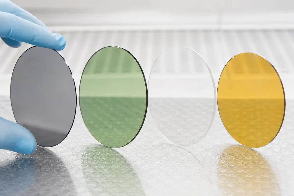
GaN-on-Si vs GaN-on-SiC vs GaN-on-sapphire vs GaN-on-GaN: GaN-on-Si leads on cost and wafer size, GaN-on-SiC leads on heat removal and crystal quality, sapphire leads in LEDs, and native GaN leads on defect density. Pick GaN-on-Si for power devices up to 650 V, GaN-on-SiC for RF, GaN-on-GaN for vertical high-voltage devices.
Key takeaways
- Lattice mismatch with GaN is about 17% on Si(111), about 16% on c-plane sapphire, about 3.5% on SiC and zero on GaN.
- Thermal expansion mismatch is worst on Si (about 54%), which makes thick GaN layers on Si prone to cracking and bow.
- SiC conducts heat at roughly 330 to 490 W/m·K, about ten times sapphire, which is why RF GaN sits on SiC.
- GaN-on-Si runs on 150 mm and 200 mm silicon lines; native GaN wafers are mostly 50 mm to 100 mm and costly.
Why GaN needs a foreign substrate
Silicon wafers are sliced from crystals pulled out of a melt. GaN cannot be made that way. At atmospheric pressure it decomposes into gallium and nitrogen before it melts, and holding it molten would need extreme nitrogen pressure. Bulk GaN is instead grown slowly by hydride vapour phase epitaxy (HVPE), ammonothermal growth or sodium-flux methods. The result is small, expensive wafers.
So for most of its history GaN has been grown as a thin film on someone else’s crystal. This is called heteroepitaxy. The substrate sets three things: how many defects the GaN film carries, how well heat escapes the device, and how much the wafer costs. For the base GaN material data, see our GaN properties table.
Substrate comparison table
Mismatch is calculated against wurtzite GaN (a = 3.189 Å; a-axis thermal expansion about 5.6 × 10⁻⁶ K-1). Lattice mismatch uses (aGaN − asub) / asub on the growth plane. Thermal mismatch uses (αGaN − αsub) / αGaN. Other conventions give slightly different percentages, so treat the figures as approximate.
| Property | Si (111) | SiC (4H/6H, semi-insulating) | Sapphire (c-plane Al2O3) | GaN (native) |
|---|---|---|---|---|
| In-plane lattice mismatch with GaN (%) | About −17 (GaN in tension) | About +3.5 (GaN in compression) | About +16 (after 30° in-plane rotation) | 0 |
| Substrate thermal expansion (10-6 K-1) | About 2.6 | About 4.2 to 4.7 | About 7.5 | About 5.6 |
| Thermal expansion mismatch (%) | About +54 (tensile on cool-down) | About +16 to +25 (tensile) | About −34 (compressive) | 0 |
| Thermal conductivity (W/m·K, 300 K) | About 130 to 150 | About 330 to 490 | About 35 to 42 | About 130 to 230 |
| Electrically | Conductive or high-resistivity | Semi-insulating (RF) or conductive | Insulating | Conductive or semi-insulating |
| Typical threading dislocation density in GaN (cm-2) | About 108 to 109 | About 108 to 109 | About 108 to 109 | About 104 to 106 |
| Typical diameters in use (status as of 2025) | 150 mm and 200 mm in production; 300 mm demonstrated | 100 mm and 150 mm | 100 mm to 150 mm (LEDs) | 50 mm common; 100 mm in limited supply |
| Main market | Power transistors, 100 V to 650 V | RF power amplifiers | LEDs and micro-LEDs | Laser diodes, vertical power research |
What is the lattice mismatch of GaN on Si?
About 17% on the Si(111) plane. The hexagonal surface of Si(111) has an in-plane spacing of about 3.84 Å, against 3.189 Å for GaN. That gap is large. Grown directly, GaN would relax by forming a dense web of dislocations.
The bigger practical problem is thermal. Growth runs at around 1,000 °C. On cool-down, GaN tries to shrink about twice as much as silicon. The film ends up in tension, the wafer bows, and thick layers crack. Gallium also reacts with silicon at growth temperature, which etches the surface in a defect called meltback.
The industry’s answer is the strain-engineered buffer. An AlN nucleation layer blocks the Ga-Si reaction. On top sit either step-graded AlGaN layers or AlN/GaN superlattices. These build in compressive strain during growth that offsets the tensile strain from cooling. A modern GaN-on-Si power stack is typically a few micrometres thick, and most of that thickness is buffer.
Which substrate is used for GaN power devices?
Silicon, for nearly all commercial GaN power transistors. The reasons are economic rather than physical:
- Cheap, large wafers. Silicon substrates cost a small fraction of SiC or GaN per unit area and come in 150 mm and 200 mm sizes that existing fabs already handle.
- Reuse of depreciated fabs. GaN-on-Si wafers can run through 150 mm and 200 mm silicon lines with added epitaxy and a gold-free process.
- Lateral devices tolerate defects. In a HEMT, current flows sideways in the 2DEG near the surface, not through the dislocated buffer. Densities of 108 to 109 cm-2 are acceptable.
The limit is voltage. The vertical voltage the buffer can hold to the silicon underneath caps practical ratings. That is why most GaN-on-Si power parts are rated at 650 V or below. For the device-level comparison with silicon MOSFETs, see GaN vs silicon, and for applications, our overview of GaN in high-power applications.
Why is GaN-on-SiC preferred for RF?
RF power amplifiers for radar, satellite links and cellular base stations dissipate high power densities in a small gate area. Junction temperature drives both output power and lifetime. Three properties make SiC the default:
- Thermal conductivity. At about 330 to 490 W/m·K, SiC pulls heat away roughly two to three times better than silicon and about ten times better than sapphire. The channel runs cooler at the same output power.
- Semi-insulating substrate. High-purity or vanadium-doped semi-insulating SiC has very high resistivity. That keeps RF losses and parasitic capacitance low at GHz frequencies. Conductive silicon would absorb signal.
- Close lattice match. At about 3.5% mismatch, GaN on SiC needs a thinner buffer and grows with less strain. Thinner buffers mean shorter heat paths and fewer trapping sites that cause current collapse.
The cost is the substrate. Semi-insulating SiC wafers cost far more than silicon and are smaller. For RF, where die are small and performance per die matters most, that trade is worth it. GaN-on-Si RF exists and targets cost-sensitive volume markets, but GaN-on-SiC remains the reference for high-power RF. Our SiC wafers guide covers substrate types and diameters.
GaN-on-sapphire: the LED workhorse
Sapphire is where GaN optoelectronics grew up. It is cheap, chemically stable at growth temperature, transparent from the UV through the visible, and available in large volumes. The lattice mismatch of about 16% is handled with a low-temperature nucleation layer, a technique that made high-quality GaN films practical in the late 1980s and early 1990s.
Its weakness is heat. At about 35 to 42 W/m·K, sapphire conducts heat worse than any other option here. That is acceptable for LEDs, where the chip can be flipped and heat removed through the top contacts, but it rules sapphire out for most high-power electronics. Sapphire’s transparency also helps deep-UV emitters, covered in our article on nitride UV LEDs.
Why is native GaN expensive?
Native GaN substrates give homoepitaxy: zero lattice mismatch, zero thermal mismatch and dislocation densities around 104 to 106 cm-2, three or more orders of magnitude lower than heteroepitaxial GaN. The catch is production.
- No melt growth. GaN decomposes before it melts, so the cheap Czochralski method used for silicon does not apply.
- Slow processes. HVPE, ammonothermal and sodium-flux growth all produce boules far shorter than a silicon ingot per run, and ammonothermal growth runs at high pressure.
- Small diameters. 50 mm wafers are the common size. 100 mm is available but in limited volume.
For now, native GaN is used where defects matter most: blue and violet laser diodes, where dislocations shorten lifetime, and vertical GaN power devices in development for ratings above 1 kV, where current flows through the full crystal thickness.
Pick X when
- Pick GaN-on-Si when you need lateral power transistors from about 100 V to 650 V at the lowest cost per die, made on large wafers in existing silicon fabs.
- Pick GaN-on-SiC when you need maximum RF output power, low RF loss and the best heat removal, and can pay for the substrate.
- Pick GaN-on-sapphire when you are making LEDs or micro-LEDs and want a cheap, transparent, insulating substrate.
- Pick GaN-on-GaN when defect density limits the device: laser diodes and vertical power devices above about 1 kV.
FAQ
Is GaN-on-SiC better than GaN-on-Si?
It is better on heat removal, crystal quality and RF loss. It is worse on cost and wafer size. For RF power, SiC usually wins. For consumer and data-centre power conversion at 650 V and below, silicon usually wins on economics.
Why does GaN grow on Si(111) and not Si(100)?
The (111) surface has threefold symmetry that matches the hexagonal base of wurtzite GaN. The (100) surface used in CMOS has fourfold symmetry, which leads to mixed-orientation, highly defective films.
What is current collapse in GaN HEMTs?
Current collapse is a temporary drop in drain current after high-voltage stress. Electrons get trapped at the surface or in the buffer and deplete the 2DEG. Buffer design and surface passivation reduce it, and thinner, cleaner buffers on SiC help.
Can GaN-on-Si reach 1,200 V?
It is difficult because the buffer must hold the full voltage vertically to the silicon. Thicker buffers, insulating substrates and native GaN are all being explored for 1,200 V-class GaN.
Sources
- Ioffe Institute, New Semiconductor Materials (NSM) archive: http://www.ioffe.ru/SVA/NSM/Semicond/
- T. Kimoto and J. A. Cooper, Fundamentals of Silicon Carbide Technology, Wiley-IEEE Press.
- U. K. Mishra, P. Parikh and Y.-F. Wu, “AlGaN/GaN HEMTs: an overview of device operation and applications,” Proceedings of the IEEE (2002).
- B. J. Baliga, Fundamentals of Power Semiconductor Devices, Springer.



