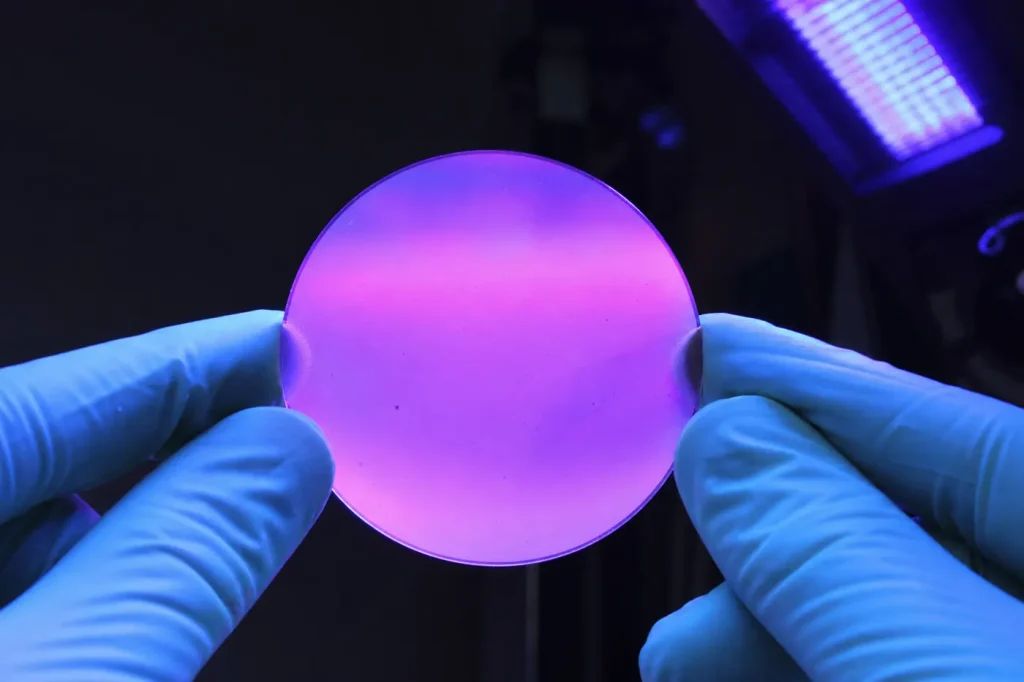
AlGaN (aluminium gallium nitride, AlxGa1−xN) is a III-nitride alloy whose bandgap can be tuned from about 3.4 eV (GaN) to about 6.1 eV (AlN) by changing the aluminium fraction. It forms the barrier layer that creates the electron channel in GaN HEMTs, and it is the active material in deep-ultraviolet LEDs.
Key takeaways
- End points at room temperature: GaN about 3.4 eV, AlN about 6.0 to 6.2 eV. The alloy gap bows below a straight line between them.
- HEMT barriers typically use 15% to 35% aluminium and are about 15 to 30 nm thick, giving a 2DEG of roughly 1013 electrons per cm².
- The channel forms without any doping. Spontaneous and piezoelectric polarisation create it.
- The emission wavelength can be set anywhere from about 365 nm down to about 210 nm, which covers UVA, UVB and UVC.
- p-type doping gets harder as aluminium rises. The magnesium acceptor deepens from roughly 0.16 to 0.2 eV in GaN to roughly 0.5 to 0.6 eV in AlN.
What is AlGaN?
AlGaN is a solid solution of aluminium nitride and gallium nitride. Both end members crystallise in the hexagonal wurtzite structure, so aluminium atoms can replace gallium atoms on the group-III sites in any proportion. The subscript x is the aluminium mole fraction. Al0.25Ga0.75N means one in four group-III sites holds aluminium.
It is almost always grown as a thin epitaxial film by metal-organic chemical vapour deposition (MOCVD) or molecular beam epitaxy (MBE). There is no commercial bulk AlGaN crystal. The film sits on GaN for transistors and on AlN or sapphire for deep-UV emitters. AlGaN belongs to the same alloy family as InGaN, which covers the visible end of the spectrum. Our gallium nitride hub covers the parent material.
How does Al content change the bandgap?
The bandgap rises with aluminium, but not linearly. The usual model is Vegard’s law with a bowing term:
Eg(x) = x·Eg(AlN) + (1−x)·Eg(GaN) − b·x(1−x)
Here b is the bowing parameter. Published values for AlGaN cluster around 0.7 to 1.0 eV, and the spread reflects strain, growth method and how the gap was measured. With a 6.1 eV AlN end point and b near 1 eV, a 25% alloy lands near 3.9 eV, and a 50% alloy near 4.5 eV. Treat these as estimates and calibrate against photoluminescence on your own films.
| Property (300 K) | GaN | Al0.25Ga0.75N (approx.) | AlN |
|---|---|---|---|
| Bandgap (eV) | About 3.4, direct | About 3.9, direct | About 6.0 to 6.2, direct |
| Band-edge wavelength (nm) | About 365 | About 320 | About 200 to 210 |
| Lattice constant a (Å) | 3.189 | About 3.17 (Vegard) | 3.112 |
| Spontaneous polarisation (C/m²) | About −0.029 | Interpolated, with bowing | About −0.081 |
| Static dielectric constant | About 8.9 to 9.5 | Between end points | About 8.5 to 9.1 |
| Main use | Channel, buffer, blue LEDs | HEMT barrier | Substrate, buffer, UVC template |
Two other properties move with composition. The a-axis lattice constant shrinks by about 2.4% from GaN to AlN, so AlGaN grown on GaN is under tensile strain. And thermal conductivity and electron mobility drop in the middle of the range, because random Al and Ga atoms scatter phonons and electrons. This alloy disorder is one reason the channel sits in the GaN, not the AlGaN.
Why is AlGaN used as the HEMT barrier?
A high-electron-mobility transistor (HEMT) needs a thin sheet of electrons, called a two-dimensional electron gas (2DEG), confined at a heterojunction. In AlGaN/GaN that sheet forms with no intentional doping. Ambacher and colleagues showed why in their 1999 and 2000 papers in the Journal of Applied Physics.
- Spontaneous polarisation. Wurtzite nitrides have a built-in dipole along the c-axis. AlN’s is almost three times GaN’s, so the step in polarisation at the interface leaves a fixed positive sheet charge on Ga-face material.
- Piezoelectric polarisation. The AlGaN is stretched to fit the larger GaN lattice. That tensile strain adds a second polarisation in the same direction, which increases the sheet charge.
- Electrons gather to balance the charge. Electrons, mainly supplied by donor-like surface states on the AlGaN, collect in a triangular quantum well on the GaN side of the interface. The conduction-band offset keeps them there.
The result is a sheet density near 1013 cm−2 with mobility around 1,500 to 2,000 cm²/V·s. That combination is what gives GaN HEMTs their low on-resistance and high current density. Our article on GaN polarisation works through the charge balance in more detail.
What Al fraction and thickness do HEMT barriers use?
Most production AlGaN/GaN HEMT barriers sit between about 15% and 35% aluminium, with 20% to 30% the most common window, and a thickness of about 15 to 30 nm. Mishra, Parikh and Wu’s 2002 Proceedings of the IEEE review describes this design space. The choice is a trade-off.
- More aluminium raises 2DEG density. Ambacher’s calculations and measurements show sheet charge rising roughly linearly with x. More charge lowers sheet resistance.
- More aluminium raises strain. Above a critical thickness the barrier relaxes or cracks, and the piezoelectric share of the charge is lost. High-Al barriers must be thinner.
- Thinner barriers give better gate control. RF devices for millimetre-wave bands scale the barrier down, and some move to AlN or InAlN barriers to keep charge high at a few nanometres.
- Below a minimum thickness, the 2DEG vanishes. A very thin barrier cannot pull enough electrons from the surface. This effect is one route to normally-off (e-mode) devices, along with p-GaN gates and recessed gates.
A thin GaN cap of a few nanometres and a SiN passivation layer usually sit on top. They stabilise the surface states that supply the 2DEG, and they matter a great deal for current collapse. For how these devices are used in power conversion, see our overview of GaN for high-power applications.
AlGaN in deep-UV LEDs and lasers
Because AlGaN keeps a direct bandgap across the full composition range, it can emit light from the near UV to about 210 nm. That covers UVA (315 to 400 nm), UVB (280 to 315 nm) and UVC (100 to 280 nm). UVC near 260 to 280 nm is the band used for germicidal disinfection, and it needs roughly 45% to 60% aluminium in the quantum wells.
Deep-UV LEDs are far less efficient than blue InGaN LEDs. Four problems stack up as aluminium rises:
- Dislocations. Films on sapphire or AlN templates carry high threading-dislocation densities, which act as non-radiative recombination centres.
- Poor p-side conduction. Covered below.
- Absorbing contacts. Designs often use a p-GaN contact layer because p-AlGaN conducts so poorly, but p-GaN absorbs UVC light.
- Light polarisation switch. At high Al content the valence-band ordering changes, and emission becomes increasingly polarised along the c-axis. That light travels sideways and is hard to extract from the top surface.
Our feature on nitride semiconductors in UV LEDs covers device structures and applications.
What limits AlGaN p-doping?
Magnesium is the only practical acceptor in the nitrides, and it is already deep in GaN. Its ionisation energy is roughly 0.16 to 0.2 eV in GaN, so only a few percent of Mg atoms release a hole at room temperature. The energy climbs with aluminium content, to roughly 0.5 to 0.6 eV in AlN. Nam and colleagues reported about 0.63 eV for Mg in AlN in Applied Physics Letters (2003). At that depth, room-temperature hole densities are tiny.
Compensation makes it worse. Native defects and hydrogen passivate or offset the acceptors, and Mg-H complexes must be broken by a post-growth anneal, as in GaN. The background of the problem is covered in our page on p-type GaN and magnesium doping.
Engineers use three workarounds:
- Polarisation doping. Grading the Al fraction along the growth direction spreads the polarisation charge through the layer. That charge pulls in holes without relying on thermal ionisation. Simon and colleagues demonstrated the effect in Science (2010).
- Superlattices. Alternating Mg-doped AlGaN layers of different composition use band bending to raise the average hole density.
- Tunnel junctions. These replace the resistive p-contact with a heavily doped junction that converts electrons to holes, so the top contact can be n-type.
n-type doping has its own ceiling. Silicon donors work well in low- and mid-Al AlGaN, but at very high Al content conductivity falls. DX-centre formation and self-compensation by cation vacancies are the usual explanations.
AlGaN against the barrier alternatives
AlGaN is the default barrier because it is mature and easy to grow on GaN by MOCVD. Two alternatives show up in RF work. InAlN at about 17% to 18% indium is lattice-matched to GaN, so it has no piezoelectric term but very strong spontaneous polarisation, and it can deliver high sheet charge from a thin, unstrained barrier. A thin AlN barrier gives the highest charge of all but is hard to grow and contact. For property data across the nitride family, see our semiconductor comparison tables.
FAQ
Is AlGaN a direct or indirect bandgap semiconductor?
Direct across the full composition range. That is unusual among wide-gap alloys and is the reason AlGaN can make deep-UV LEDs and lasers.
Why is the AlGaN/GaN 2DEG called undoped?
Because the electrons come from polarisation charge and surface states, not from donor atoms in the barrier. Some designs add silicon doping, but the channel forms without it.
What happens if the AlGaN barrier is too thick?
Above a critical thickness, set by Al content, the strained film relaxes through dislocations or cracks. The piezoelectric contribution falls and the 2DEG density drops.
What Al content gives a 265 nm emitter?
Roughly half aluminium in the quantum wells, with higher-Al barriers around them. The exact value depends on well width, strain and the bowing parameter, so growers calibrate it by photoluminescence.
Sources
- O. Ambacher et al., “Two-dimensional electron gases induced by spontaneous and piezoelectric polarization charges in N- and Ga-face AlGaN/GaN heterostructures,” Journal of Applied Physics (1999); and the follow-up on undoped and doped AlGaN/GaN heterostructures, Journal of Applied Physics (2000).
- U. K. Mishra, P. Parikh and Y.-F. Wu, “AlGaN/GaN HEMTs: an overview of device operation and applications,” Proceedings of the IEEE (2002).
- Ioffe Institute, New Semiconductor Materials (NSM) archive, entries for GaN, AlN and AlGaN.
- K. B. Nam, M. L. Nakarmi, J. Li, J. Y. Lin and H. X. Jiang, “Mg acceptor level in AlN probed by deep ultraviolet photoluminescence,” Applied Physics Letters (2003).
- J. Simon, V. Protasenko, C. Lian, H. Xing and D. Jena, “Polarization-induced hole doping in wide-band-gap uniaxial semiconductor heterostructures,” Science (2010).



