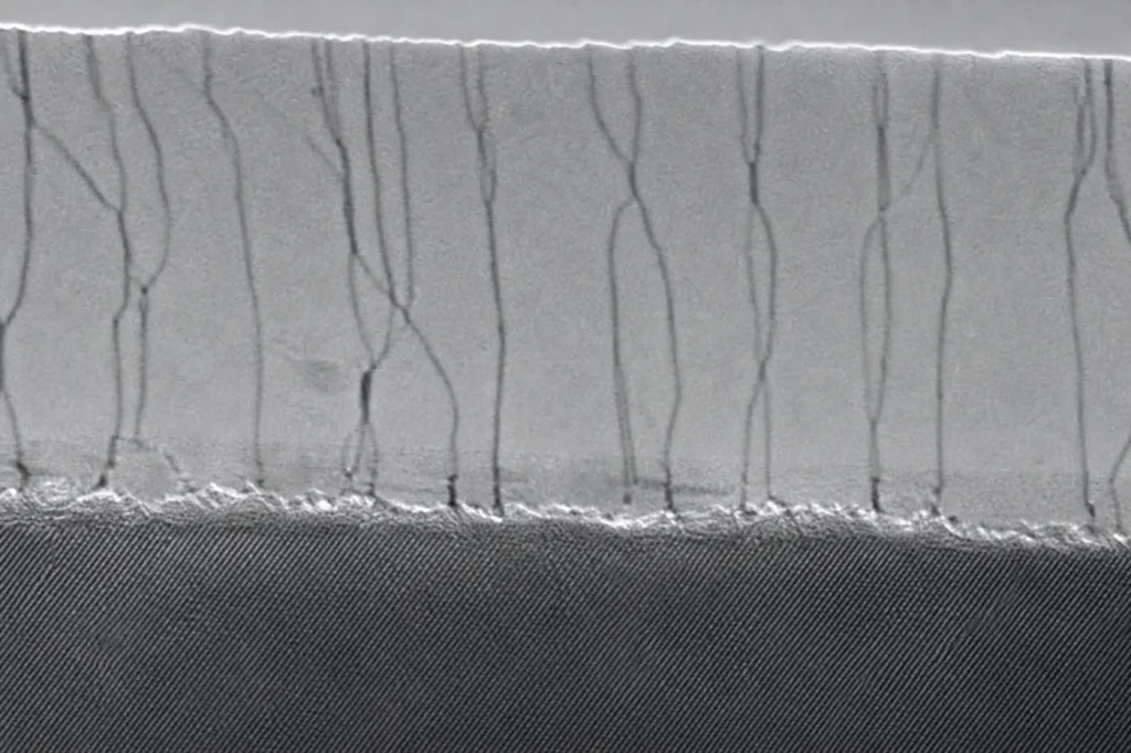
Defects in GaN are breaks in the ideal wurtzite crystal, dominated by threading dislocations: line defects that run up through the film from the substrate interface. Heteroepitaxial GaN on sapphire, SiC or silicon typically carries about 108 to 109 cm−2. Bulk native GaN substrates bring that down to roughly 104 to 106 cm−2.
Key takeaways
- GaN is mostly grown on foreign substrates with 3.5 % to 17 % lattice mismatch, which seeds threading dislocations.
- Typical threading dislocation density (TDD): about 108 to 109 cm−2 on sapphire, SiC and Si; about 106 to 107 cm−2 in ELOG wing regions; about 104 to 106 cm−2 on bulk GaN.
- InGaN LEDs stay efficient at densities that would kill a GaAs LED, mainly because indium fluctuations and V-pits keep carriers away from dislocation cores.
- Dislocations hurt most where current or field is concentrated: Schottky and gate leakage, laser diode lifetime and vertical power devices.
- Epitaxial lateral overgrowth (ELOG) cuts density by orders of magnitude above masked regions.
Why does GaN have so many dislocations?
A dislocation is a line along which the atomic planes of a crystal are misaligned. A threading dislocation runs from the substrate interface up through the epitaxial layer, roughly along the growth direction, and ends at the surface. Each one is a line of distorted bonds that can trap carriers, scatter them or conduct leakage current.
GaN has many because it is almost always grown on something else. Large, cheap native GaN wafers did not exist when the industry formed, so growers used sapphire, then SiC and silicon. All three differ from GaN in lattice constant and in thermal expansion.
- Sapphire (0001): about 16 % in-plane mismatch after the 30° lattice rotation.
- SiC (0001): about 3.5 %.
- Si (111): about 17 %, plus a large thermal expansion difference that puts the film in tension on cooling.
Growth starts as separate islands that are slightly tilted and twisted against each other. Where islands merge, the misalignment is taken up by dislocations. Because the wurtzite c-axis is the growth direction and the main glide systems do not let these lines bend away easily, most of them thread straight up. Our GaN crystal structure guide covers the substrate orientations.
The breakthrough that made device-quality GaN on sapphire possible was the low-temperature nucleation layer. Amano, Akasaki and co-workers introduced a low-temperature AlN buffer in 1986. Nakamura later developed a low-temperature GaN buffer. These layers set up a well-oriented starting surface and brought densities down into the range where LEDs worked.
Types of threading dislocations
Dislocations are classified by their Burgers vector, b, the lattice displacement they carry.
- Edge (a-type): b = ⅓⟨11−20⟩. Usually the most common type in c-plane films.
- Screw (c-type): b = ⟨0001⟩. Less common, but often linked to leakage paths and surface spiral growth.
- Mixed (a+c type): b = ⅓⟨11−23⟩. Combines both; frequently implicated in reverse leakage.
Other defects matter too. Point defects include gallium vacancies and carbon and oxygen impurities; some are tied to the broad yellow luminescence near 2.2 eV seen in many GaN films. Basal-plane stacking faults are common in nonpolar and semipolar GaN. Inversion domains, regions of flipped polarity, appear under some growth conditions and at heavy Mg doping.
What dislocation density is typical on sapphire vs native GaN?
| Substrate or method | Lattice mismatch to GaN | Typical TDD (cm−2) | Main uses |
|---|---|---|---|
| Sapphire, standard MOCVD | About 16 % | About 108 to 109 (up to 1010 in poor material) | LEDs, the volume leader |
| SiC | About 3.5 % | About 108 to 109 | RF HEMTs, some LEDs |
| Si (111) | About 17 % | About 108 to 109, often the upper end | Power HEMTs, some LEDs and RF |
| ELOG on sapphire (wing regions) | Same template | About 106 to 107 | Laser diodes |
| Free-standing GaN from HVPE | Native | About 105 to 106 | Laser diodes, vertical power devices |
| Ammonothermal bulk GaN | Native | About 104 to 105 in good material | Research and premium substrates |
| Reference: GaAs or Si wafers | Native | Below about 104; Si essentially dislocation-free | Mainstream electronics |
The substrate choice is mostly an economics and thermal question; see GaN-on-Si vs GaN-on-SiC for that trade-off.
Why do GaN LEDs work despite defects?
This was the surprise of the 1990s. In GaAs and other III-V emitters, densities above roughly 104 to 105 cm−2 sharply cut efficiency and lifetime. Lester and co-workers reported in 1995 that bright InGaN LEDs operated with dislocation densities near 1010 cm−2. Three explanations are widely accepted.
- Carrier localisation. Indium in InGaN quantum wells is not perfectly uniform. Potential minima from composition and thickness fluctuations trap electrons and holes before they diffuse to a dislocation.
- Short diffusion length. Carrier diffusion lengths in GaN are short, of the order of 100 nm or less, compared with the typical spacing between dislocations at 108 cm−2 (about 1 µm). Many carriers recombine before reaching a defect.
- V-pits. Dislocations that reach the quantum-well region open small hexagonal pits with thinner, wider-gap sidewall wells. Hangleiter and co-workers showed in Physical Review Letters (2005) that this creates an energy barrier that keeps carriers away from the dislocation core.
Defects still matter in LEDs. Lower TDD improves efficiency at low current, ultraviolet LEDs (where localisation is weaker), and long-term reliability. For more on the InGaN active region, see our InGaN guide.
Impact on leakage and reliability
- Schottky and gate leakage. Screw and mixed dislocations are linked to conductive paths under Schottky contacts. In HEMTs, that raises gate leakage and can affect off-state breakdown.
- Current collapse and trapping. Dislocations and point defects in the buffer trap charge under high drain bias, which temporarily raises on-resistance. Buffer engineering, often with carbon or iron doping, is used to control this.
- Laser diode lifetime. Laser diodes run at much higher current density than LEDs. Nakamura’s group found that continuous-wave lifetimes improved substantially once lasers were grown on low-dislocation ELOG and later on free-standing GaN.
- Vertical power devices. Vertical GaN diodes and transistors put the full blocking field across the drift layer. Dislocations there become leakage paths and early-breakdown sites, so vertical GaN power devices are built on bulk GaN wafers. See our overview of GaN for high-power applications.
How are defects reduced (ELOG)?
Epitaxial lateral overgrowth (ELOG), also called ELO or LEO, is a regrowth method that blocks threading dislocations with a mask. The steps are:
- Grow a GaN template on sapphire, SiC or Si.
- Deposit a dielectric mask, usually SiO2 or SiNx, and open stripe windows a few micrometres wide.
- Regrow GaN. It starts in the windows, then grows sideways over the mask.
- Dislocations in the windows continue upward, but material over the mask, the “wings”, grows laterally from the window edge and is largely free of threading dislocations.
Wing regions reach about 106 to 107 cm−2, a reduction of two to three orders of magnitude. The drawbacks are extra process steps, non-uniform density across the wafer and new defects where adjacent wings meet. Laser stripes are aligned over the wings. Related methods include pendeo-epitaxy, patterned sapphire substrates (now standard for LEDs, where they also improve light extraction) and in-situ SiNx interlayers that cause dislocations to bend and annihilate.
The long-term answer is native substrates. HVPE free-standing wafers and ammonothermal crystals give the lowest densities, at higher cost and smaller diameter. For a broader property view of GaN, see the gallium nitride hub, and compare it with other materials in our comparison tables.
FAQ
What is a good threading dislocation density for GaN?
It depends on the device. LEDs and lateral HEMTs work well at about 108 to 109 cm−2. Laser diodes and vertical power devices aim for 106 cm−2 or lower.
How is dislocation density measured?
Common methods are X-ray diffraction rocking-curve widths, plan-view transmission electron microscopy, cathodoluminescence dark-spot counting, atomic force microscopy of surface pits and defect-selective etching.
Does GaN-on-silicon have more dislocations than GaN-on-sapphire?
Often slightly more, at the upper end of the 108 to 109 cm−2 range, because of larger mismatch and tensile stress. Modern buffers narrow the gap.
Sources
- S. D. Lester et al., “High dislocation densities in high efficiency GaN-based light-emitting diodes,” Applied Physics Letters (1995).
- A. Hangleiter et al., “Suppression of nonradiative recombination by V-shaped pits in GaInN/GaN quantum wells produces a large increase in the light emission efficiency,” Physical Review Letters (2005).
- H. Amano, I. Akasaki and co-workers on low-temperature AlN buffer layers (1986), and S. Nakamura and co-workers on low-temperature GaN buffers and ELOG-based InGaN laser diodes.
- S. M. Sze and K. K. Ng, Physics of Semiconductor Devices, 3rd ed., Wiley.
- Ioffe Institute, New Semiconductor Materials (NSM) archive, GaN entry.



