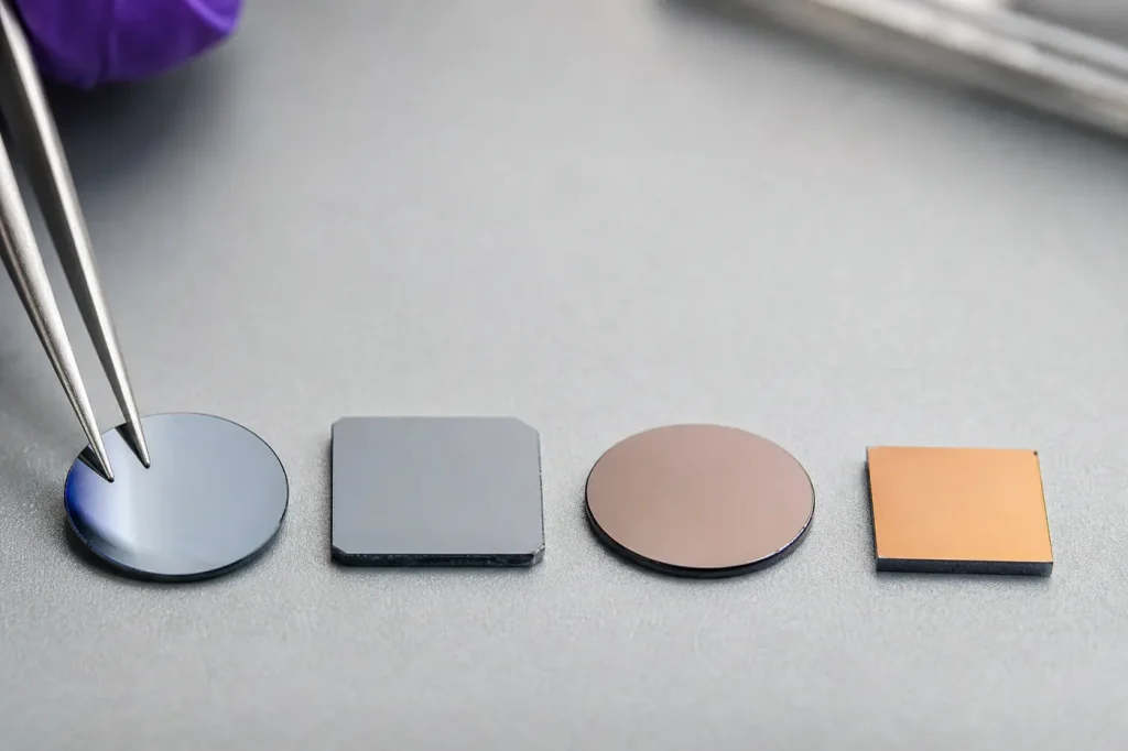
The CS Fusion Semiconductor Materials Index is one reference table for the semiconductors that matter in industry and research: elemental silicon and germanium, plus III-V, IV-IV, II-VI, oxide, 2D and organic compounds. Start here for a material’s class, bandgap and crystal structure, then follow the link to its full guide.
Key takeaways
- Silicon (1.12 eV, indirect) is the baseline. Every other material here earns its place by beating silicon on one specific number.
- Wide-bandgap materials, SiC (about 3.26 eV) and GaN (3.39 eV), carry roughly ten times silicon’s critical field, which is why they lead in power electronics.
- Direct-gap materials such as GaAs, InP and GaN emit light efficiently. Indirect-gap Si, Ge and SiC do not.
- Pick the hub by application: power, RF, photonics, logic or flexible electronics.
Key numbers at 300 K
Bandgap is the energy an electron needs to break free of its bond and carry current. A direct gap lets the material emit light efficiently; an indirect gap mostly does not. All values are at 300 K, about room temperature.
| Material | Class | Bandgap (eV, 300 K) | Gap type | Crystal structure |
|---|---|---|---|---|
| Silicon (Si) | Elemental, group IV | 1.12 | Indirect | Diamond cubic |
| Germanium (Ge) | Elemental, group IV | 0.66 | Indirect | Diamond cubic |
| Silicon carbide (4H-SiC) | IV-IV compound | 3.23 to 3.26 | Indirect | Hexagonal (4H polytype) |
| Silicon-germanium (Si1-xGex) | IV-IV alloy | 0.66 to 1.12, set by Ge fraction | Indirect | Diamond cubic |
| Gallium arsenide (GaAs) | III-V | 1.42 | Direct | Zincblende |
| Indium phosphide (InP) | III-V | 1.34 | Direct | Zincblende |
| Gallium nitride (GaN) | III-V (III-nitride) | 3.39 | Direct | Wurtzite |
| Gallium phosphide (GaP) | III-V | 2.26 | Indirect | Zincblende |
| Zinc oxide (ZnO) | II-VI | 3.37 | Direct | Wurtzite |
| Gallium oxide (β-Ga2O3) | Oxide | About 4.8 to 4.9 | Disputed (direct and indirect gaps nearly equal) | Monoclinic |
| Molybdenum disulfide (MoS2), monolayer | 2D (transition metal dichalcogenide) | About 1.8 to 1.9 (bulk about 1.2 to 1.3) | Direct as monolayer, indirect in bulk | Hexagonal, layered |
| Pentacene | Organic (small molecule) | About 1.8 to 2.2 (optical) | — | Triclinic molecular crystal |
What are the main semiconductor materials?
Semiconductors fall into two groups. Elemental semiconductors are made of one element: silicon and germanium, both from group IV of the periodic table. Compound semiconductors combine two or more elements, usually from groups that average out to four valence electrons per atom. Our explainer on what a compound semiconductor is covers the chemistry, and the basics of compound semiconductors walks through each class.
The compound classes used today are III-V (GaAs, InP, GaN), II-VI (ZnO, CdTe), IV-IV (SiC, SiGe), oxides (Ga2O3), layered 2D materials (MoS2) and carbon-based organics. Silicon still makes up the large majority of chips by volume. Compound semiconductors take the jobs where silicon’s physics runs out: high voltage, high frequency and light emission. For the classification rules, see the types of semiconductor.
Which are elemental and which are compound?
Only group IV supplies useful elemental semiconductors: silicon, germanium and, at the extreme, diamond (about 5.5 eV). Tin is semimetallic in its grey form and metallic in its white form. Everything else in the table is a compound or an alloy. A compound has a fixed ratio of elements, such as one gallium to one arsenic in GaAs. An alloy, such as Si1-xGex or InxGa1-xAs, lets the ratio slide, and the bandgap and lattice constant slide with it.
That tunability is the practical reason compounds exist in industry. A device designer can choose a composition to hit a target emission wavelength or to match the lattice of a substrate. Silicon offers one bandgap only. The trade-off is cost: compound wafers are smaller and harder to grow, and some ingredients, such as arsenic and phosphorus, need careful handling. Our list of semiconductor examples groups materials by class, and what a semiconductor is made of covers the raw materials.
Which materials are wide-bandgap?
A wide-bandgap semiconductor has a gap well above silicon’s 1.12 eV. Thresholds of about 2 eV and about 3 eV both appear in the literature; our guide to wide-bandgap semiconductors explains where the line is drawn. The commercial pair is 4H-SiC (about 3.26 eV) and GaN (3.39 eV). Ultra-wide-bandgap candidates include β-Ga2O3 (about 4.8 eV), diamond (about 5.5 eV) and AlN (about 6.2 eV).
Why it matters: critical field, the electric field a material holds before it breaks down, rises steeply with bandgap. Silicon manages about 0.3 MV/cm. SiC and GaN reach about 2.5 to 3.3 MV/cm. A tenfold field means a much thinner drift layer for the same voltage, which cuts resistance and switching loss. That is the core of the advantages of compound semiconductors in power electronics.
Direct or indirect: which materials emit light?
In a direct-gap material, an electron can drop across the gap and release a photon without help. In an indirect-gap material, the electron also needs a lattice vibration to conserve momentum, so light emission is weak. That single distinction explains why LEDs and lasers are built from GaAs, InP, GaN and their alloys, and almost never from silicon.
The III-V family covers most direct-gap materials in production. See what III-V semiconductors are for the members and their emission wavelengths, and examples of compound semiconductors for a wider list.
Which material page answers my question?
Start from the job, not the material. For power switches at 1,200 V and above, including EV inverters, go to silicon carbide. For compact converters at 650 V and below, and for high-power RF, go to gallium nitride. For phone RF front ends, VCSELs and space solar cells, go to gallium arsenide. For 1.3 µm and 1.55 µm telecom lasers and photodiodes, go to indium phosphide.
For RF transistors built on standard silicon lines, see silicon-germanium. For atom-thin channels, see 2D semiconductors. For flexible displays and printed electronics, see organic semiconductors, and for solution-processed solar and emitters, perovskites and quantum dots. Head-to-head trade-offs live in comparisons. If you are new to the field, what materials are semiconductors sets out the criteria.
Start here
- What is a Compound Semiconductor
- What Is a Wide-Bandgap Semiconductor?
- What Are III-V Semiconductors? Members, Properties and Uses
All materials guides
Definitions and classification
- What is a Compound Semiconductor
- Understanding the Basics of Compound Semiconductors
- What Are III-V Semiconductors? Members, Properties and Uses
- What Is a Wide-Bandgap Semiconductor?
- What are types of semiconductor?
Examples
FAQs
- What materials are semiconductors?
- What is a semiconductor made of?
- What are the advantages of compound semiconductors?
Related material hubs
- Gallium nitride (GaN)
- Silicon carbide (SiC)
- Gallium arsenide (GaAs)
- Indium phosphide (InP)
- Silicon-germanium (SiGe)
- 2D semiconductors
- Organic semiconductors
- Perovskites and quantum dots
- Material comparisons
FAQ
What is the most widely used semiconductor material?
Silicon. It has a moderate 1.12 eV bandgap, a stable native oxide (SiO2) and 300 mm wafers, which together make it the cheapest material for logic and memory.
Is gallium nitride a compound semiconductor?
Yes. GaN combines gallium from group III with nitrogen from group V, so it is a III-V compound and a member of the III-nitride family with AlN and InN.
What bandgap counts as wide?
There is no single cut-off. Most sources call a material wide-bandgap above about 2 eV, and the commercial wide-bandgap materials, SiC and GaN, sit near 3.3 eV.
Sources
- Ioffe Institute, New Semiconductor Materials (NSM) archive, http://www.ioffe.ru/SVA/NSM/Semicond/
- S. M. Sze and K. K. Ng, Physics of Semiconductor Devices, 3rd ed., Wiley.
- T. Kimoto and J. A. Cooper, Fundamentals of Silicon Carbide Technology, Wiley-IEEE Press.
