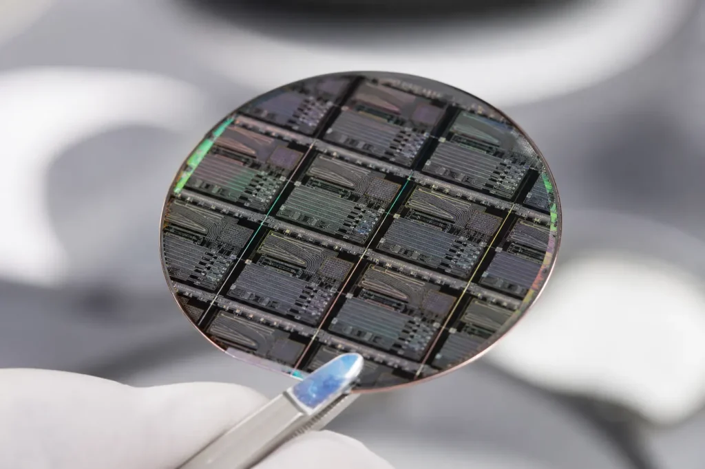
Indium phosphide (InP) is a III-V compound semiconductor with a direct bandgap of 1.34 eV at 300 K. Its main value is as a substrate: InGaAs and InGaAsP alloys grown on InP emit and detect light at 1.3 µm and 1.55 µm, the low-loss windows of optical fibre, so InP underpins telecom and data-centre photonics.
Key takeaways
- Bandgap 1.34 eV, direct; InP itself emits near 0.92 µm, but alloys lattice-matched to it reach 1.3 to 1.65 µm.
- In0.53Ga0.47As on InP absorbs out to about 1.7 µm and carries very fast electrons.
- Device types: DFB and EML lasers, modulators, photodiodes, photonic integrated circuits and HBTs.
- Versus GaAs: smaller, costlier wafers, but the only practical platform for long-wavelength lasers.
Key numbers at 300 K
Values are for undoped InP at 300 K, with GaAs alongside because the two are often weighed against each other.
| Property (300 K) | InP | GaAs (reference) |
|---|---|---|
| Crystal structure | Zincblende (cubic) | Zincblende (cubic) |
| Lattice constant (Å) | 5.869 | 5.653 |
| Bandgap (eV) | 1.34, direct | 1.42, direct |
| Band-edge wavelength (µm) | About 0.92 | About 0.87 |
| Electron mobility (cm²/V·s) | Up to about 5,400 | Up to about 8,500 |
| Hole mobility (cm²/V·s) | Up to about 200 | Up to about 400 |
| Electron effective mass (m0) | About 0.08 | 0.063 |
| Critical field (MV/cm) | About 0.5 | About 0.4 |
| Thermal conductivity (W/m·K) | About 68 | About 55 |
| Static dielectric constant | 12.5 | 12.9 |
| Density (g/cm³) | 4.81 | 5.32 |
What is indium phosphide?
InP combines indium from group III with phosphorus from group V in a zincblende crystal. Its lattice constant, 5.869 Å, is the reason it matters: a set of ternary and quaternary alloys (InGaAs, InGaAsP, InAlAs) can be grown on it without strain, and those alloys have exactly the bandgaps telecom needs. InP wafers can be made semi-insulating by iron doping, which isolates high-speed devices.
The wafers are small, typically 50 mm to 100 mm in diameter, and brittle, which keeps cost high. See the basics of InP, InP’s material properties and InP wafers and Fe-doped substrates.
Why is InP used for telecom lasers?
Silica fibre loses least light near 1.55 µm and has near-zero dispersion near 1.31 µm. A laser at those wavelengths needs an active layer with a bandgap of about 0.8 to 0.95 eV. InGaAsP grown lattice-matched on InP covers that span, while InP’s own wider gap (1.34 eV) makes it a transparent, low-index cladding that confines light and current. Silicon cannot do this job: its indirect gap makes it a poor light emitter, so silicon photonics needs bonded III-V material for its lasers.
On InP the industry builds DFB lasers (distributed feedback, single wavelength), EMLs (electro-absorption modulated lasers), Mach-Zehnder modulators and photonic integrated circuits (PICs) that place lasers, modulators and detectors on one chip. See InP in photonics and high-speed electronics.
What is InGaAs on InP?
In0.53Ga0.47As is the composition of indium gallium arsenide that matches InP’s lattice exactly. Its bandgap is about 0.75 eV, so it absorbs light out to about 1.7 µm. That makes it the standard absorber in telecom PIN photodiodes, avalanche photodiodes and short-wave infrared image sensors.
The same alloy carries electrons with mobility above 10,000 cm²/V·s, so it forms the channel of InP HEMTs and the base of InP HBTs. These transistors serve the fastest circuits in optical transceivers and millimetre-wave systems, and research InP HEMTs have reported maximum oscillation frequencies above 1 THz.
The cost of that speed is voltage. InGaAs has a narrow gap, so InP transistors break down at a few volts, far below GaN. InP electronics therefore sit where bandwidth matters more than power: transimpedance amplifiers and drivers inside optical modules, and receivers and low-noise amplifiers at millimetre-wave and sub-terahertz frequencies.
How is InP made?
Bulk InP melts at about 1,060 °C, and at that temperature phosphorus has a very high vapour pressure. Crystals are therefore grown under pressure: liquid-encapsulated Czochralski (LEC) pulls a seed through a melt capped with boron oxide inside a high-pressure chamber, while vertical gradient freeze (VGF) cools a sealed melt from the bottom for lower defect density. Iron doping makes the substrate semi-insulating; sulphur or zinc make it n-type or p-type.
Device structures are grown by MOCVD or MBE. Lasers need quantum wells only a few nanometres thick, and their composition must hold the lattice match to InP within a small fraction of a percent, or the strain creates defects that shorten laser life. Fabrication then adds gratings for DFB lasers, ridge waveguides and passivation. Processing is mostly done on small wafers in dedicated fabs, a key reason InP chips cost more per square millimetre than silicon or GaAs.
How does InP compare with GaAs?
GaAs has higher electron mobility (about 8,500 vs 5,400 cm²/V·s), larger and cheaper wafers, and owns the 850 nm and 940 nm VCSEL market for short-reach links and sensing. InP wins on wavelength reach: 1.3 µm and 1.55 µm lasers for metro, long-haul and data-centre links can only be grown practically on InP. InP also conducts heat slightly better (about 68 vs 55 W/m·K) and has a higher critical field.
Rule of thumb: short-reach and high-volume, pick GaAs; long-reach optics and the highest transistor speeds, pick InP. More head-to-heads are in our comparisons section; for context, see III-V semiconductors and the materials index.
Start here
- Exploring the Basics of Indium Phosphide (InP)
- Understanding Indium Phosphide and its Role in Semiconductors
- Understanding Indium Phosphide: An Overview
All indium phosphide guides
Basics, properties and wafers
- Exploring the Basics of Indium Phosphide (InP)
- Understanding Indium Phosphide as a Semiconductor Material
- Understanding Indium Phosphide: An Overview
Photonics and high-speed electronics
Compound semiconductor background
- Understanding the Basics of Compound Semiconductors
- What is a Compound Semiconductor
- What Are III-V Semiconductors? Members, Properties and Uses
- What Is a Wide-Bandgap Semiconductor?
- Semiconductors Examples
FAQs
- What materials are semiconductors?
- What are types of semiconductor?
- What are the advantages of compound semiconductors?
- What is a semiconductor made of?
- What are examples of compound semiconductors?
Related material hubs
FAQ
What wavelength does InP emit?
Bulk InP emits near 0.92 µm, set by its 1.34 eV gap. Telecom lasers on InP use InGaAsP or InGaAlAs active layers to emit at 1.3 µm or 1.55 µm.
Is indium phosphide toxic?
The International Agency for Research on Cancer classifies InP as probably carcinogenic to humans (Group 2A), so fabs control dust from wafer grinding and dicing. Phosphine gas used in epitaxy is also highly toxic.
Why not make telecom lasers in silicon?
Silicon’s indirect gap makes it a very weak light emitter, and its 1.12 eV gap is transparent at 1.55 µm. Silicon photonics therefore bonds InP-based material onto silicon for the laser.
Sources
- Ioffe Institute, New Semiconductor Materials (NSM) archive, http://www.ioffe.ru/SVA/NSM/Semicond/
- S. M. Sze and K. K. Ng, Physics of Semiconductor Devices, 3rd ed., Wiley.
- L. A. Coldren, S. W. Corzine and M. L. Mašanović, Diode Lasers and Photonic Integrated Circuits, 2nd ed., Wiley.
