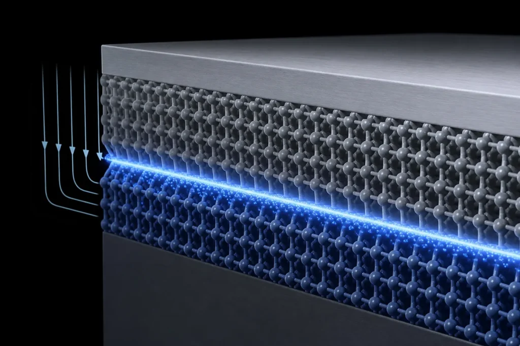
GaN polarization is a built-in electric dipole in wurtzite nitride crystals that exists without any applied voltage. It has two parts: spontaneous polarization from the crystal’s asymmetry and piezoelectric polarization from strain. At AlGaN/GaN interfaces it creates electron sheets near 1013 cm−2 without doping, and in InGaN quantum wells it weakens light emission.
Key takeaways
- Spontaneous polarization (PSP) comes from wurtzite’s lack of inversion symmetry. Calculated values: GaN −0.029, AlN −0.081, InN −0.032 C/m² (Bernardini, Fiorentini and Vanderbilt, 1997).
- Piezoelectric polarization (PPE) comes from strain. AlGaN grown on GaN is under tension, and its piezoelectric term adds to the spontaneous term.
- The jump in total polarization at the AlGaN/GaN interface leaves a fixed positive sheet charge. Electrons gather there to form a two-dimensional electron gas (2DEG) of about 1013 cm−2.
- In c-plane InGaN quantum wells, the same effect produces fields of the order of 1 MV/cm. This is the quantum-confined Stark effect (QCSE).
- Nonpolar and semipolar crystal planes remove or reduce these fields.
Why does GaN have built-in polarization?
Polarization is the electric dipole moment per unit volume of a material, measured in C/m². Most cubic semiconductors, such as silicon and GaAs, have none at rest, because their symmetry cancels it out. Wurtzite GaN is different.
Wurtzite has a unique polar axis, the c-axis, and no centre of inversion. The Ga–N bonds are partly ionic, with charge pulled toward nitrogen. In an ideal tetrahedron the dipoles of the four bonds would cancel. In real GaN, the c/a ratio (about 1.626) and the internal parameter u differ slightly from the ideal, so the dipoles do not cancel along the c-axis. The leftover is spontaneous polarization, PSP. It is present in an unstrained crystal at equilibrium.
The sign convention follows the crystal. For Ga-polar GaN, grown along [0001], PSP points toward the substrate. Flip to N-polar growth and the direction reverses. Our guide to GaN crystal structure explains polarity in detail.
AlN deviates most from the ideal wurtzite shape, so it has the largest spontaneous polarization of the three nitrides, roughly three times that of GaN. For GaN’s other material properties, see our gallium nitride hub.
Polarization constants for the nitrides
| Constant | GaN | AlN | InN |
|---|---|---|---|
| Spontaneous polarization PSP (C/m²) | −0.029 | −0.081 | −0.032 |
| Piezoelectric constant e33 (C/m²) | 0.73 | 1.46 | 0.97 |
| Piezoelectric constant e31 (C/m²) | −0.49 | −0.60 | −0.57 |
| Lattice constant a (Å) | 3.189 | 3.112 | 3.545 |
These numbers are large. For comparison, the piezoelectric e33 of GaN is several times that of GaAs. That is why polarization dominates the electrostatics of nitride heterostructures.
What is piezoelectric polarization in AlGaN/GaN?
Piezoelectric polarization, PPE, is extra polarization caused by strain. Squeeze or stretch the crystal and the bond geometry changes, shifting the dipole balance. In a c-plane layer with biaxial in-plane strain, the piezoelectric term along the c-axis is:
PPE = 2·[(a − a0)/a0]·(e31 − e33·C13/C33)
Here a is the strained in-plane lattice constant, a0 the relaxed value, and C13 and C33 are elastic constants. For the nitrides, the bracketed material term is always negative.
In practice: AlxGa1−xN has a smaller lattice constant than GaN. A thin AlGaN barrier grown on a thick GaN buffer is stretched in-plane to match GaN. That tensile strain gives a negative PPE, the same sign as PSP. In Ga-polar AlGaN/GaN, the two contributions add. InGaN on GaN is the reverse: it is compressed, and its piezoelectric term opposes its spontaneous term, with the piezoelectric part usually larger.
How does polarization create a 2DEG?
Where polarization changes abruptly, it leaves a fixed bound charge. At an interface the sheet charge equals the difference in total polarization:
σ = (PSP + PPE)GaN − (PSP + PPE)AlGaN
For Ga-polar AlGaN on GaN, AlGaN has the more negative total polarization, so σ is positive. Ambacher and co-workers showed in their 1999 Journal of Applied Physics paper that this bound charge is of the order of 1013 electron charges per cm² for typical aluminium fractions, and that it matches the measured electron densities in N-face and Ga-face structures.
The positive sheet charge pulls electrons to the GaN side of the interface. The conduction band bends below the Fermi level in a thin triangular well, a few nanometres wide. Electrons confined there form a two-dimensional electron gas (2DEG): free to move in the plane, quantised normal to it. Typical figures for an Al0.25Ga0.75N to Al0.3Ga0.7N barrier about 20 to 30 nm thick are a sheet density of roughly 0.8 to 1.5 × 1013 cm−2 and room-temperature mobility of about 1,500 to 2,000 cm²/V·s.
Where do the electrons come from? Not from dopants. The widely accepted explanation, set out by Ibbetson and co-workers in 2000, is that donor-like states at the AlGaN surface give up their electrons to the channel. The 2DEG density therefore depends on barrier thickness: below a critical thickness of a few nanometres, no 2DEG forms.
This is the basis of the GaN high electron mobility transistor (HEMT). Because the channel exists at zero gate bias, a standard AlGaN/GaN HEMT is normally on (depletion mode). Making it normally off takes extra work, such as a p-GaN gate or a recessed barrier. The device consequences are covered in our GaN vs SiC comparison and our overview of GaN for high-power applications. Heterojunction band diagrams are explained in junctions, contacts and diodes.
What is the quantum-confined Stark effect?
The quantum-confined Stark effect (QCSE) is the change in quantum-well energy levels and wavefunctions caused by an electric field across the well. In c-plane InGaN/GaN light emitters, the field comes from the polarization difference between the well and the barriers. For blue and green compositions it is reported in the range of about 1 MV/cm and above, rising with indium content.
The field tilts the bands across the well. Electrons are pushed to one side and holes to the other. Three effects follow:
- Red shift. The effective transition energy falls below the flat-band value, so the well emits at a longer wavelength than its composition alone suggests.
- Lower radiative rate. Electrons and holes overlap less, so they recombine radiatively more slowly. Non-radiative paths win a larger share, cutting efficiency. The effect grows with well width, which is why InGaN wells are kept thin, typically 2 to 3 nm.
- Blue shift with current. Injected carriers partly screen the field as current rises. The emission wavelength moves shorter, a familiar trait of green InGaN LEDs.
QCSE gets worse as indium content rises, so it is one of the reasons green InGaN LEDs are less efficient than blue ones. See our InGaN guide for the wider green gap story.
How to reduce or use polarization
- Nonpolar planes. On m-plane or a-plane GaN, the c-axis lies in the growth plane. Waltereit and co-workers reported m-plane GaN/AlGaN quantum wells free of electrostatic fields in Nature in 2000.
- Semipolar planes. Inclined planes such as (20−21) reduce the field while keeping good indium uptake.
- Polarization-matched barriers. Quaternary AlInGaN barriers can be tuned to match the well’s polarization, shrinking the interface charge.
- Polarization doping. Grading AlGaN composition spreads the bound charge through a volume, which pulls in mobile carriers without dopant atoms. This is used to make p-type and n-type layers in wide-gap AlGaN.
FAQ
Does silicon or GaAs have spontaneous polarization?
No. Their cubic diamond and zincblende structures are too symmetric along the usual growth directions. GaAs is piezoelectric under some strains, but far weaker than GaN.
Why is a standard GaN HEMT normally on?
The 2DEG forms from polarization charge at zero gate bias. A negative gate voltage is needed to deplete it, unless the gate stack is redesigned for enhancement mode.
Does polarization flip in N-polar GaN?
Yes. Reversing the crystal reverses the polarization vectors. In N-polar AlGaN/GaN, the 2DEG forms in GaN grown on top of the AlGaN instead of below it.
Are the polarization constants measured or calculated?
The most cited spontaneous values are first-principles calculations. Direct measurement is hard, so device modelling usually starts from Bernardini and co-workers or Ambacher and co-workers and calibrates against measured 2DEG densities.
Sources
- F. Bernardini, V. Fiorentini and D. Vanderbilt, “Spontaneous polarization and piezoelectric constants of III-V nitrides,” Physical Review B (1997).
- O. Ambacher et al., “Two-dimensional electron gases induced by spontaneous and piezoelectric polarization charges in N- and Ga-face AlGaN/GaN heterostructures,” Journal of Applied Physics (1999), with a follow-up on undoped and doped structures in Journal of Applied Physics (2000).
- J. P. Ibbetson et al., work on surface donor states as the source of 2DEG electrons in AlGaN/GaN, Applied Physics Letters (2000).
- P. Waltereit et al., “Nitride semiconductors free of electrostatic fields for efficient white light-emitting diodes,” Nature (2000).
- Ioffe Institute, New Semiconductor Materials (NSM) archive, GaN entry.



