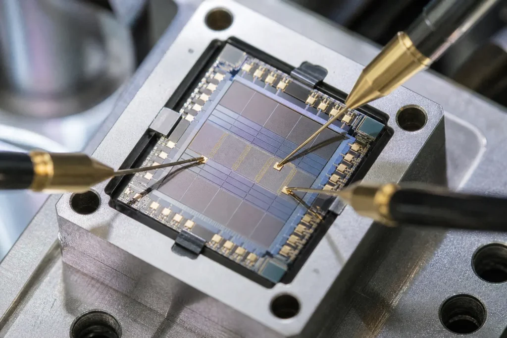
A junction is an interface inside a device where two materials, or two differently doped regions, meet. A p-n junction and a Schottky metal-semiconductor contact both rectify, passing current one way. An ohmic contact conducts both ways with low resistance. A heterojunction joins two semiconductors with different bandgaps.
Key takeaways
- Built-in potential rises with doping and with bandgap: about 0.7 V in Si and about 1.2 V in GaAs for 1016 cm-3 on each side.
- Schottky diodes carry majority carriers only, so they switch fast with no reverse-recovery charge.
- Ohmic contacts rely on heavy doping under the metal, so carriers tunnel through a thin barrier.
- The AlGaN/GaN heterojunction forms a two-dimensional electron gas without doping: the channel of the GaN HEMT.
p-n vs Schottky vs ohmic vs heterojunction
| Feature | p-n junction | Schottky contact | Ohmic contact | Heterojunction |
|---|---|---|---|---|
| What meets | p-type and n-type regions | Metal and semiconductor | Metal and heavily doped semiconductor | Two semiconductors with different Eg |
| Barrier origin | Built-in potential Vbi from doping | Barrier φB ≈ φm − χ, modified by Fermi-level pinning | Barrier thin enough to tunnel, or near zero | Band offsets ΔEC and ΔEV |
| Rectifying? | Yes | Yes | No: linear I-V | Depends on doping and offsets |
| Current carried by | Minority carriers (diffusion) | Majority carriers (thermionic emission) | Majority carriers | Device dependent; 2DEG electrons in a HEMT |
| Forward drop (Si) | About 0.6 to 0.7 V | About 0.2 to 0.5 V | Near 0 V | — |
| Switching | Slower: stored minority charge | Fast: no minority storage | Not applicable | Fast in HEMTs |
| Typical devices | Rectifiers, LEDs, solar cells, BJTs | Schottky diodes, SiC power diodes, HEMT gates | Source, drain, anode and cathode contacts | HEMTs, HBTs, laser diodes |
What is a p-n junction?
Put p-type and n-type material in contact and electrons diffuse into the p side while holes diffuse into the n side. They recombine and leave behind fixed ionised dopants: positive on the n side, negative on the p side. This depletion region holds an electric field that stops further diffusion. The potential across it is the built-in potential, Vbi.
Band diagram: EF is flat across the junction. EC and EV sit higher on the p side and bend down through the depletion region by qVbi. Forward bias lowers that step and current rises exponentially. Reverse bias raises it and only a small leakage flows until breakdown.
Vbi = (kT/q) ln(NAND/ni2). Because ni falls exponentially with bandgap, wider-gap materials give larger Vbi. With 1016 cm-3 on each side, the formula gives about 0.72 V for Si, about 1.2 V for GaAs and close to 3 V for 4H-SiC. See How pn junction is formed?, What is pn junction diode? and the doping hub.
What is a Schottky barrier?
A Schottky barrier forms where a metal meets a moderately doped semiconductor. In the ideal Schottky-Mott picture, the barrier height for electrons is φB = φm − χ: metal work function minus semiconductor electron affinity. In practice, interface states pin the Fermi level and the barrier depends less on the metal than this rule predicts.
Band diagram: for an n-type semiconductor, the bands bend upward toward the metal, forming a depletion region on the semiconductor side only. The metal’s Fermi level lines up with the semiconductor’s EF. Current flows by thermionic emission of majority electrons over the barrier.
No minority charge is stored, so Schottky diodes switch quickly and drop less voltage than a p-n diode of the same material. The cost is higher reverse leakage. SiC Schottky diodes are standard in power supplies because SiC’s critical field keeps leakage and drift thickness in check; see silicon carbide, breakdown field compared and What are the types of diode?.
What is an ohmic contact?
An ohmic contact passes current in both directions with a linear current-voltage curve and low resistance. It is quoted as specific contact resistivity, in Ω·cm². Most metal-semiconductor pairs form a barrier, so engineers dope the semiconductor heavily, typically above about 1019 cm-3, directly under the metal.
Band diagram: the barrier is still there, but the depletion region is only a few nanometres thick. Electrons tunnel through it instead of climbing over. Contacts to wide-gap p-type material, such as p-GaN, are hard because the barrier is large and heavy p-doping is limited; see p-type GaN and What is the resistivity of a semiconductor?.
What is a 2DEG?
A heterojunction joins two semiconductors with different bandgaps. Their band edges do not line up, so steps appear: ΔEC in the conduction band and ΔEV in the valence band. Electrons collect on the low-EC side in a thin triangular well. When that well dips below EF, the confined electrons form a two-dimensional electron gas (2DEG), free to move along the interface but not across it.
Band diagram: EC drops sharply at the interface, forming a narrow well whose bottom lies below the flat EF. In AlGaAs/GaAs the electrons come from doping placed in the AlGaAs, away from the channel. In AlGaN/GaN, polarisation charge induces a sheet density of about 1013 cm-2 without doping, at mobilities of about 1,500 to 2,000 cm²/V·s.
A transistor on this channel is a high-electron-mobility transistor (HEMT). Read GaN polarisation and the 2DEG, the gallium nitride hub, the gallium arsenide hub and bandgap engineering. Band offsets start from the values in the Energy Bands hub.
All junction and diode guides
Diodes and junctions
- What is pn junction diode?
- How pn junction is formed?
- What are the types of diode?
- What is the advantage of diode?
- Is diode a semiconductor?
- What is the most basic semiconductor device?
Semiconductor fundamentals
General semiconductor FAQs
- What are the main advantages of semiconductors over metals?
- Why are semiconductors special?
- Are semiconductors easily damaged by high temperature?
- What are the disadvantages of semiconductor?
- What are the advantages and disadvantages of semiconductor devices?
- What is the resistivity of a semiconductor?
- What is the principle of semiconductor?
- What are the 3 properties of semiconductors?
Related physics hubs
FAQ
Why does a Schottky diode have a lower forward voltage than a p-n diode?
Its barrier is set by the metal-semiconductor interface and is usually lower than the built-in potential of a p-n junction in the same material. Current is carried by majority carriers emitted over that barrier, so less forward bias is needed for the same current.
What is the difference between a Schottky contact and an ohmic contact?
Both are metal-semiconductor contacts. A Schottky contact has a wide depletion region and rectifies. An ohmic contact uses heavy doping to make the barrier thin enough to tunnel through, so it conducts both ways with low resistance.
Does a p-n junction need two different materials?
No. A homojunction uses one semiconductor with p-type and n-type doping, as in a silicon diode. A heterojunction uses two semiconductors with different bandgaps, such as AlGaAs on GaAs or AlGaN on GaN.
Sources
- S. M. Sze and K. K. Ng, Physics of Semiconductor Devices, 3rd ed., Wiley.
- C. Kittel, Introduction to Solid State Physics, 8th ed., Wiley.
- Ioffe Institute, New Semiconductor Materials (NSM) archive, http://www.ioffe.ru/SVA/NSM/Semicond/
