Infineon said on Nov. 9, 2026 that it has made working silicon carbide (SiC) power devices on 300 mm wafers at its Villach, Austria fab, using existing manufacturing equipment. The news arrives as NVIDIA and its power partners prepare 800 VDC power distribution for 1 MW-class AI racks, with the rollout starting in 2027.
What happened
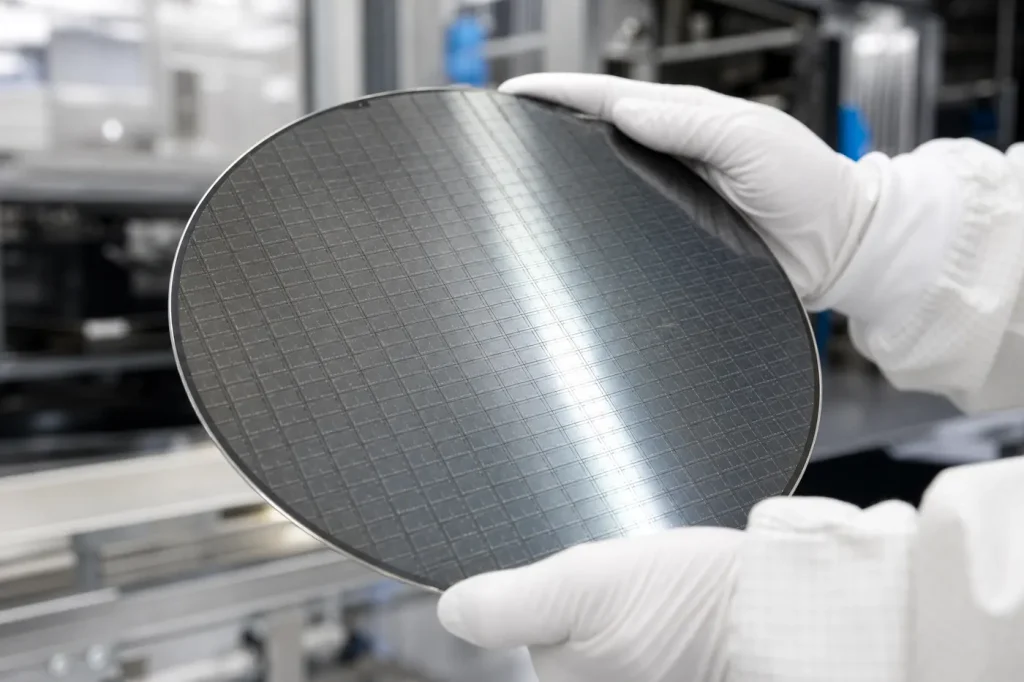
According to Infineon’s November 2026 press release, as reported by electrive on Nov. 10, 2026, the company produced functional SiC power devices on 300 mm wafers under industrial fab conditions. Infineon says a 300 mm wafer yields about 2.3 times as many chips as a 200 mm wafer.
The claim is about devices, not substrates. Wolfspeed announced a 300 mm single-crystal SiC wafer in January 2026, according to Igor’s Lab coverage. Infineon’s “world first” covers working devices made in a production fab. Secondary coverage also reports that Infineon’s Cold Split wafer-separation method works for 300 mm SiC at its Dresden site. No date has been announced for commercial 300 mm SiC production.
On the demand side, NVIDIA’s technical blog of May 20, 2025 says the company is leading a move to 800 VDC to support 1 MW IT racks and beyond, starting in 2027. Its silicon partners are Analog Devices, Infineon, Innoscience, MPS, Navitas, onsemi, Renesas, ROHM, STMicroelectronics and TI. Delta, Flex Power, Lead Wealth, LiteOn and Megmeet supply power-system components, and Eaton, Schneider Electric and Vertiv cover data center power. Tom’s Hardware reports that ABB later announced its support.
Why it matters for SiC and GaN power devices
This section is CS Fusion’s analysis. Infineon did not tie its 300 mm result to 800 VDC; it is separately one of NVIDIA’s 800 VDC silicon partners. We read the two together because they meet in the same product: high-voltage power switches for AI racks.
800 VDC raises the voltage class. At 1 MW, a 48 V bus carries about 20,800 A; an 800 V bus carries 1,250 A. Conduction loss scales with current squared, which is the case for going higher. Switches on an 800 V bus need headroom above it, which points to the 1,200 V class. That is SiC’s core range, as our GaN vs SiC comparison shows. Stages that step down to lower voltages inside the rack can use 650 V-class and low-voltage parts, where GaN’s fast switching shrinks magnetics. NVIDIA’s partner list includes suppliers known for SiC, for GaN, and for both.
300 mm is a cost lever, not yet a supply change. SiC device volume today runs on 150 mm wafers, with 200 mm ramping; see our SiC wafers guide. Infineon’s 2.3x chip count per wafer spreads fixed processing cost over more die. Substrate cost and crystal defect density still weigh heavily on SiC device cost, and a working device on 300 mm says little yet about yield at that size. For the material basics, see our silicon carbide hub.
What we don’t know yet
- When, or whether, Infineon will move SiC production to 300 mm. No date has been announced.
- Device type, voltage class and yield of the 300 mm devices. The coverage we checked does not give them.
- Where 300 mm SiC substrates will come from in volume.
- Whether the 2027 start for 800 VDC holds. NVIDIA describes a roadmap, not a completed shift.
- How conversion stages in 800 VDC racks will split between SiC and GaN. No partner has published a full bill of materials.
Sources
- Infineon, press release infpr202611-028, November 2026: https://www.infineon.com/press-release/2026/infpr202611-028
- electrive, “Infineon processes SiC on 300 mm wafers for the first time”, Nov. 10, 2026: https://www.electrive.com/2026/11/10/infineon-processes-sic-on-300-mm-wafers-for-the-first-time/
- NVIDIA Technical Blog, “NVIDIA 800 V HVDC Architecture Will Power the Next Generation of AI Factories”, May 20, 2025: https://developer.nvidia.com/blog/nvidia-800-v-hvdc-architecture-will-power-the-next-Generation-of-ai-factories
- Tom’s Hardware, on ABB supporting NVIDIA’s 800 VDC rollout, date not shown: https://www.tomshardware.com/tech-industry/big-tech/nvidia-800-vdc-power-rollout-for-1-megawatt-server-racks-to-be-supported-by-abb-company-says-collaboration-will-create-new-power-solutions-for-future-gigawatt-scale-data-centers