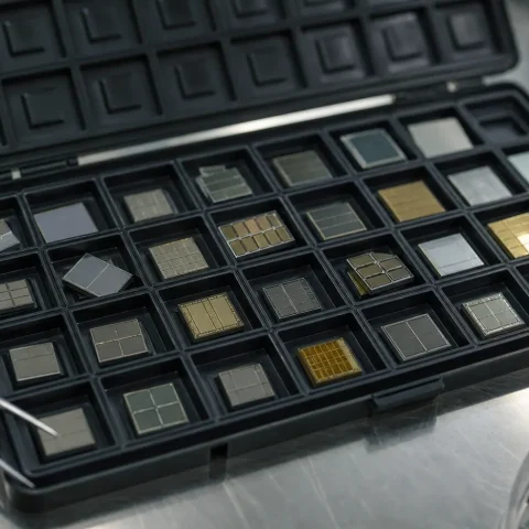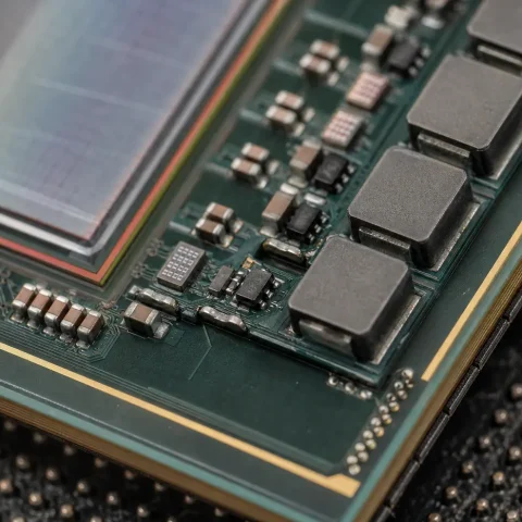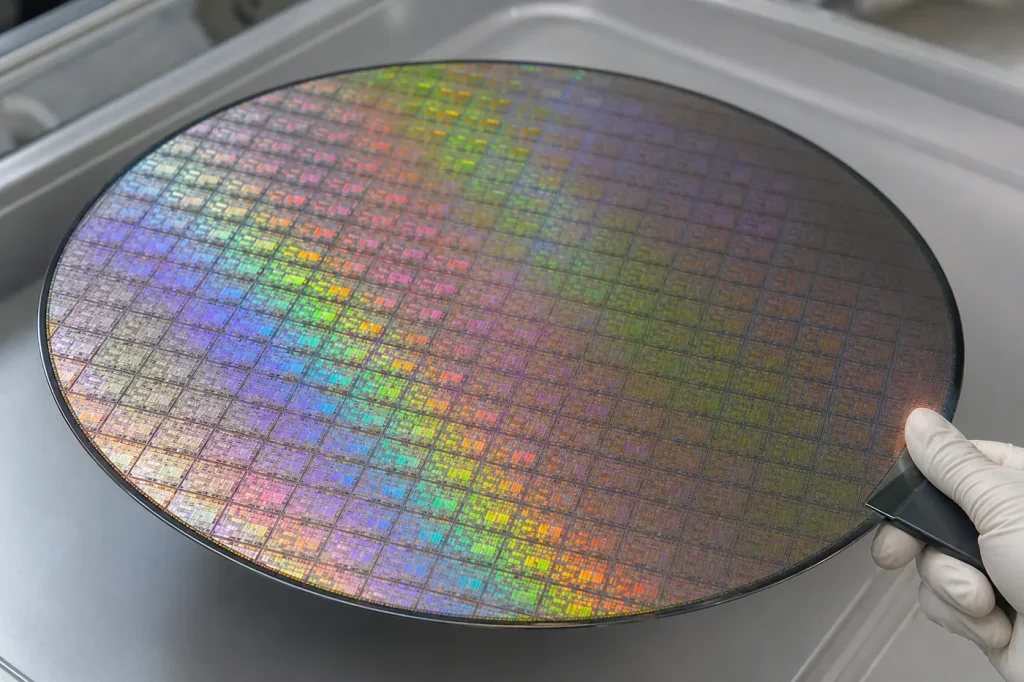
Intel Foundry made the process design kit (PDK) 0.9 for its 14A process generally available in late October 2026, according to the Intel newsroom, and is targeting PDK 1.0 in the first quarter of 2027. Elon Musk has said the Terafab chip project plans to use 14A, though Intel’s role there is not locked in.
What happened
An Intel newsroom explainer, published without a date in late October or early November 2026, announces general availability of 14A PDK 0.9 and gives Q1 2027 as the target for PDK 1.0. Tom’s Hardware reported the same milestones.
Intel’s page gives no date for high-volume manufacturing (HVM). Secondary reports point to risk production in the second half of 2027 and HVM in 2028. The Elec has reported mass production in 2029. None of these dates comes from Intel.
On Terafab, Intel said on Apr. 7, 2026 that it had joined the project with SpaceX, xAI and Tesla. On Tesla’s Q1 2026 earnings call, Musk said: “We plan to use Intel’s 14A process.” DCD covered his comments. That plan is not settled. A SpaceX IPO filing reportedly says neither Tesla nor Intel is required to stay in the project, and Musk has confirmed talks with TSMC about Terafab, according to Tom’s Hardware. Tesla and SpaceX cite about $16.8 billion for phase one. Media estimates of $20 billion to $25 billion are unconfirmed.
Why it matters for compound semiconductor engineers
This section is CS Fusion’s analysis.
What a 0.9 PDK means. A PDK is the package a foundry gives chip designers: design rules, transistor and interconnect models, parameterised cells and the files that plug into EDA tools. A version below 1.0 means the models are close to final but can still shift. Customers can start real designs on 0.9; most will not commit production tape-outs until 1.0. Q1 2027 is therefore the date that matters for first 14A customer silicon.
Silicon logic sets the load for compound devices. No GaN, SiC or InP device will be built on 14A. But each new logic node packs more compute into a package, and that package is what the power chain and the optical links must serve. Higher current at sub-1 V core rails puts pressure on the final conversion stages, where gallium nitride competes with silicon at 48 V and below. Faster chip-to-chip traffic pushes demand for optical links built on indium phosphide lasers. A credible second leading-edge foundry, alongside TSMC, would widen where those AI processors are made, not what they need from the power and optical side.
For the device physics behind these trade-offs, see our physics section.
What we don’t know yet
- When 14A reaches HVM. Intel has not said; outside reports range from 2028 to 2029.
- Which external customers are designing on PDK 0.9. Intel’s page does not name them.
- Whether Terafab will use 14A at all. Musk has said it plans to, but Intel’s participation is not contractually locked in and TSMC is also in talks.
- Terafab’s real cost. The $16.8 billion phase-one figure comes from Tesla and SpaceX; larger media estimates are unconfirmed.
Sources
- Intel Newsroom, “What Is the Intel 14A PDK 0.9, and Why Does It Matter to Foundry Customers?”, late October or early November 2026 (no date on page): https://www.intel.com/content/www/us/en/newsroom/news/intel-foundry/what-is-the-intel-14a-pdk-0-9-and-why-it-matters.html
- Tom’s Hardware, “Intel 14A moves closer to production as PDK 0.9 becomes available”, date not shown: https://www.tomshardware.com/tech-industry/semiconductors/intel-14a-moves-closer-to-production-as-pdk-0-9-becomes-available-process-design-kit-gives-developers-important-production-milestone-ahead-of-1-0-in-2027
- DCD, “Elon Musk says Tesla will use Intel 14A technology at its $20bn TeraFab project in Austin”, date not shown: https://www.datacenterdynamics.com/en/news/elon-musk-says-tesla-will-use-intel-14a-technology-at-its-20bn-terafab-project-in-austin/
- Tom’s Hardware, on Musk confirming Terafab talks with TSMC, date not shown: https://www.tomshardware.com/tech-industry/semiconductors/elon-musk-confirms-discussions-with-tsmc-about-terafab-chipmaking-collaboration-intel-is-the-only-other-named-partner-terafab-to-exclusively-supply-tesla-spacex-and-xai