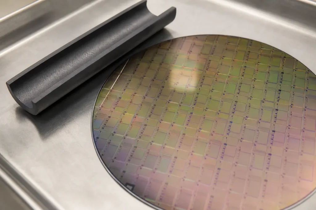
Doping silicon carbide is a two-route process, epitaxial in-situ doping and ion implantation, that replaces the thermal diffusion used in silicon. Dopants barely move in SiC below about 1,800 °C. Nitrogen and phosphorus make n-type material, aluminium makes p-type, and implants need a 1,600 to 1,800 °C anneal to become electrically active.
Key takeaways
- Diffusion coefficients of N and Al in SiC are negligible at normal processing temperatures, so selective doping uses implantation.
- Donors in 4H-SiC: nitrogen at about 0.06 and 0.12 eV (two lattice sites), phosphorus at similar or slightly shallower levels.
- The main acceptor, aluminium, sits about 0.2 eV above the valence band. Boron is deeper, at roughly 0.3 eV or more.
- High-dose implants are done hot, at a few hundred °C, and activated at about 1,600 to 1,800 °C under a carbon cap.
- p-type SiC is resistive because the acceptor is deep and hole mobility is low, about 100 cm²/V·s against about 1,000 for electrons.
Why can’t SiC be doped by diffusion?
In silicon, engineers deposit a dopant source on the surface and heat the wafer to about 900 to 1,100 °C. Dopant atoms hop through the lattice and form a junction a few microns deep. That process is called thermal diffusion, and it built the silicon industry. Our article on doping techniques in silicon covers how it works there.
SiC does not allow it. The Si-C bond is short and strong, and the lattice has very few native vacancies at moderate temperatures. Kimoto and Cooper report that the diffusion coefficients of nitrogen and aluminium are extremely small even near 1,800 °C. A useful junction would need temperatures where the SiC surface itself starts to decompose. Boron diffuses faster than other dopants, which is one reason it is avoided where sharp profiles matter.
The slow diffusion has an upside. Once a dopant is placed, it stays put through every later high-temperature step. Profiles defined by implantation survive annealing almost unchanged. So SiC device makers have two tools:
- In-situ doping during epitaxy for uniform layers: the drift layer, buffer layers and some p-type layers. See our guide to SiC epitaxy.
- Ion implantation for local regions: MOSFET p-wells, n+ source regions, p+ body contacts, junction termination and JBS diode grids.
Which dopants are used in SiC?
4H-SiC has two inequivalent lattice sites for each atom, called hexagonal (h) and cubic (k). A dopant on each site has a slightly different ionisation energy, so values usually come in pairs. The ionisation energy is the energy needed to free the dopant’s electron or hole into the band. The lower it is, the more dopants are active at room temperature.
| Dopant | Type | Lattice site | Ionisation energy in 4H-SiC (meV) | Main use |
|---|---|---|---|---|
| Nitrogen (N) | Donor | Carbon | About 60 (h) and about 120 (k) | Substrates, epi doping, n+ implants |
| Phosphorus (P) | Donor | Silicon | About 50 to 60 (h) and about 90 to 120 (k) | Low-resistance n+ implants |
| Aluminium (Al) | Acceptor | Silicon | About 190 to 230 | p-wells, p+ contacts, termination, p-type epi |
| Boron (B) | Acceptor | Silicon (shallow) or carbon-related (deep) | About 280 to 390 shallow; deep centre near 600 | Limited; some termination and research uses |
| Vanadium (V) | Deep level | Silicon | Mid-gap | Semi-insulating substrates for RF |
Nitrogen dominates n-type doping because it is easy to add from N2 gas during growth and it is the impurity that makes commercial wafers conductive. Phosphorus is preferred for some heavily doped implanted regions because it can reach lower sheet resistance at very high doses. For a general primer on donors, acceptors and ionisation, see our doping and carriers section.
Not every SiC wafer is meant to conduct. GaN-on-SiC RF transistors need a semi-insulating substrate, so that the wafer itself does not add parasitic capacitance and loss under the device. Suppliers make these wafers in two ways. One adds vanadium, which pins the Fermi level near mid-gap and traps stray carriers. The other, called high-purity semi-insulating (HPSI), keeps shallow impurities very low and relies on intrinsic point defects to compensate what remains. Either way, the target is resistivity many orders of magnitude above a conductive power substrate.
How ion implantation is done in SiC
Implantation fires ionised dopant atoms at the wafer with energies from tens of keV to a few MeV. Because the dopants will not diffuse afterwards, the final profile must be built during implant. Engineers stack several implants at different energies and doses to make a flat “box” profile to the required depth. Deep p-wells for high-voltage MOSFETs often need MeV energies.
- Hot implantation. For high doses, the wafer is held at a few hundred °C, commonly around 300 to 600 °C, during implant. The heat lets the lattice repair itself as damage forms and prevents an amorphous layer. Amorphised SiC does not recrystallise cleanly to 4H and may form 3C-SiC.
- Room-temperature implants are used for lower doses, such as channel and well implants.
- Channelling. Ions can travel deep along open crystal directions. The 4° off-cut and wafer tilt during implant are used to control this tail.
What anneal temperature activates implants?
An implanted atom is not yet a dopant. It must move onto a substitutional lattice site, and the damage around it must heal. In SiC this takes an activation anneal at about 1,600 to 1,800 °C, usually in argon, for minutes to tens of minutes. Kimoto and Cooper give this range as standard practice. Silicon needs about 1,000 °C for the same job.
At those temperatures, silicon evaporates preferentially from the surface. Without protection, the surface roughens through step bunching and loses material. The standard fix is a carbon cap: a photoresist layer baked into graphite before the anneal and removed afterwards by oxidation. The cap keeps the surface smooth enough for a good gate oxide.
Activation is not complete in every case. Nitrogen and phosphorus implants activate well. Aluminium is harder, especially at high doses, and a fraction remains inactive. Residual implant damage also leaves deep levels that cut carrier lifetime and mobility in the implanted region. This is why p+ implanted layers in SiC have higher sheet resistance than designers would like.
Why is p-type SiC resistive?
Three factors combine.
- Deep acceptor. Aluminium at about 0.2 eV is roughly eight times the thermal energy at room temperature (about 0.026 eV). Only a minority of acceptors are ionised at 300 K in heavily doped material. Nitrogen donors, at about half that depth, are mostly ionised at moderate doping.
- Low hole mobility. The Ioffe archive lists hole mobility in 4H-SiC at about 100 to 120 cm²/V·s in lightly doped material, against roughly 900 to 1,000 cm²/V·s for electrons. Mobility falls further at high doping.
- Incomplete implant activation, covered above.
The consequences show up across the device stack. Ohmic contacts to p-type SiC are harder to make than n-type contacts. p-type SiC substrates are far more resistive than n-type wafers, which is one reason commercial devices are built on n-type substrates. It also makes SiC IGBTs, which need a p-type collector, difficult to manufacture. Interestingly, ionisation rises with temperature, so p-type resistance can fall as a device heats up.
How SiC doping compares with silicon and GaN
Silicon is the easy case: shallow dopants near 0.045 eV, fast diffusion and low-temperature activation. GaN is harder than SiC on the p-side, because its magnesium acceptor is similar in depth but implant activation of Mg in GaN is far less mature. SiC sits between them. It is the only wide-bandgap material where selective n-type and p-type implantation are both in volume production. For side-by-side material data, see our comparison tables and the silicon carbide hub.
FAQ
What makes commercial SiC wafers n-type?
Nitrogen added during bulk crystal growth, to roughly 1018 to 1019 cm−3. It gives the substrate the low resistivity a vertical power device needs.
Why is a carbon cap needed for SiC annealing?
At 1,600 to 1,800 °C silicon leaves the surface faster than carbon, and the surface roughens. A graphite cap blocks that loss and keeps the surface flat for later oxidation.
Why are SiC implants done at high temperature?
Heating the wafer during high-dose implants lets damage anneal as it forms. A room-temperature high-dose implant can amorphise the surface, and amorphous SiC does not regrow cleanly as 4H-SiC.
Is boron used as a p-type dopant in SiC?
Rarely in production. It is deeper than aluminium, it forms a second deep centre and it diffuses more readily. Aluminium is the standard choice.
Sources
- T. Kimoto and J. A. Cooper, Fundamentals of Silicon Carbide Technology, Wiley-IEEE Press, chapters on doping, ion implantation and device processing.
- Ioffe Institute, New Semiconductor Materials (NSM) archive, SiC entry: impurity levels and carrier mobility.
- S. M. Sze and K. K. Ng, Physics of Semiconductor Devices, 3rd ed., Wiley.
- B. J. Baliga, Fundamentals of Power Semiconductor Devices, Springer.



