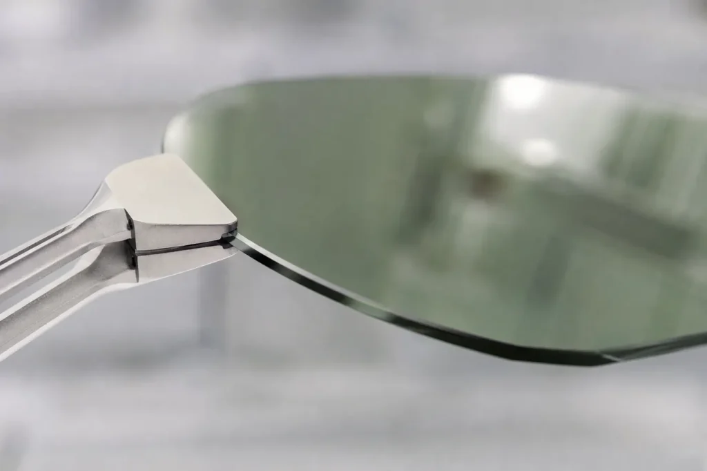
A SiC wafer is a single-crystal silicon carbide substrate, almost always the 4H polytype, sliced from a boule grown by physical vapour transport. Production runs on 150 mm wafers, with 200 mm ramping. Quality is judged by crystal defects: micropipes, now below about 1 cm−2, and basal plane dislocations, which cause bipolar degradation.
Key takeaways
- Commercial SiC substrates come in 100 mm, 150 mm and 200 mm diameters. 150 mm is the volume workhorse; 200 mm gives about 1.78 times the area per wafer.
- Power-device wafers are n-type 4H-SiC cut about 4° off the c-axis so epitaxial layers grow by step flow and keep the 4H stacking.
- Micropipes kill devices outright. Basal plane dislocations (BPDs) are subtler: under forward current they spread into stacking faults that raise on-state voltage.
- SiC wafers cost far more than silicon because growth runs above 2,000 °C, boules grow slowly and stay short, and the crystal is nearly as hard as diamond to slice and polish.
What sizes are SiC wafers?
SiC substrate diameters have stepped up from 50 mm and 76 mm in the early commercial years to 100 mm, then 150 mm, and now 200 mm. Each step took years, because a larger diameter means growing a larger defect-free seed and controlling temperature gradients across a wider crystal. Silicon moved to 300 mm long ago; SiC is roughly two generations behind in diameter.
| Diameter | Wafer area (cm²) | Area vs 150 mm | Typical thickness | Status |
|---|---|---|---|---|
| 100 mm | ~79 | 0.44× | ~350 µm | Legacy; still used for RF and research |
| 150 mm | ~177 | 1× | ~350 µm | Main production diameter for power devices |
| 200 mm | ~314 | 1.78× | ~500 µm | In early volume production at several suppliers |
The 1.78 times area gain understates the benefit. Edge exclusion takes a fixed ring at the rim, so a larger wafer loses a smaller share of its area, and per-wafer processing costs in the fab do not rise in proportion to area. The catch is that early 200 mm material has tended to carry higher defect densities than mature 150 mm material. Supplier dates and volumes change quickly, so we do not list them here; check each supplier’s current announcements.
How SiC wafers are made
SiC does not melt at practical pressures; it sublimes. So it cannot be pulled from a melt like silicon. The standard method is physical vapour transport (PVT), also called seeded sublimation or modified Lely growth. SiC powder in a graphite crucible is heated above about 2,200 °C. It sublimes, and the vapour recrystallises on a slightly cooler SiC seed crystal. The full process is covered in our explainer How is SiC made?
- Boule growth by PVT at a rate of a fraction of a millimetre per hour, giving boules only a few centimetres long.
- Shaping and orientation, cutting the flat or notch and setting the 4° off-axis angle toward the [11-20] direction.
- Slicing with diamond wire or laser-based splitting. Laser splitting reduces kerf loss, the material lost to the cut.
- Grinding, lapping and chemical-mechanical polishing to an epi-ready surface on the Si face.
- Epitaxy by chemical vapour deposition, usually done by the device maker or an epi supplier, to grow the lightly doped drift layer.
Power substrates are doped n-type with nitrogen, with resistivity typically around 0.015–0.025 Ω·cm. RF substrates for GaN-on-SiC transistors are semi-insulating instead. Our GaN-on-Si vs GaN-on-SiC comparison explains why RF uses them.
SiC wafer defects: micropipes, TSDs and BPDs
Defect density is the main quality metric for a SiC wafer. Four types matter most. Densities below are typical ranges for modern commercial 4H-SiC as described by Kimoto and Cooper; individual supplier specifications vary.
| Defect | What it is | Typical density in modern substrates | Device impact |
|---|---|---|---|
| Micropipe | Hollow-core screw dislocation with a large Burgers vector, running along the c-axis | Below ~1 cm−2; many grades near zero | Fatal: causes low-voltage breakdown in any device it crosses |
| Threading screw dislocation (TSD) | Screw dislocation along the c-axis, Burgers vector of one unit cell height | ~102–103 cm−2 | Can raise leakage and reduce oxide reliability |
| Threading edge dislocation (TED) | Edge dislocation along the c-axis | ~103–104 cm−2 | Considered relatively benign |
| Basal plane dislocation (BPD) | Dislocation lying in the (0001) basal plane | ~102–104 cm−2 in substrate; far lower in good epilayers | Drives bipolar degradation |
What is a micropipe?
A micropipe is a hollow tube, typically sub-micron to a few microns across, that runs through the crystal along the growth axis. It forms around a screw dislocation whose Burgers vector is so large that the strain energy is lower with the core opened up. Micropipes were the defect that held SiC back in the 1990s. Densities have since fallen by orders of magnitude, and they no longer limit yield in good material.
What is a basal plane dislocation?
A basal plane dislocation is a line defect lying in the hexagonal basal plane rather than along the growth axis. In 4H-SiC, a BPD splits into two partial dislocations bounding a thin ribbon of faulted stacking. On its own it does little. The problem starts when electrons and holes recombine at it.
Bipolar degradation explained
When a SiC PiN diode, or the body diode of a SiC MOSFET, conducts forward current, electrons and holes recombine in the drift layer. Energy released at a BPD lets one of its partial dislocations glide. As it moves, it leaves behind a single Shockley stacking fault, a sheet where the 4H stacking sequence is locally wrong. The fault can grow into a triangle or band spanning the whole drift layer.
The stacking fault acts as a quantum-well-like barrier to current and a trap for carriers. The result is a forward-voltage drift: VF rises over hours of bipolar operation, and the device can run hotter and fail its specification. This matters most for inverters that use the MOSFET body diode during dead time.
The industry has two main defences:
- BPD-to-TED conversion. Growth conditions at the substrate-epi interface turn most substrate BPDs into harmless threading edge dislocations as the epilayer grows. Mature processes convert the large majority of them.
- Recombination-enhancing buffer layers. A thick, heavily doped buffer between substrate and drift layer makes minority carriers recombine before they reach any remaining BPDs.
Device makers also screen with high-current stress tests, and some designs add an external Schottky diode so the body diode carries less current.
Why are SiC wafers expensive?
A SiC substrate costs many times more than a silicon wafer of the same diameter. We do not quote a ratio because prices are negotiated and move quickly, but the causes are structural:
- Extreme growth temperature. PVT runs above about 2,200 °C in graphite hot zones that wear out.
- Slow growth, short boules. A silicon Czochralski ingot can be well over a metre long. A SiC boule is a few centimetres, grown over days.
- Hardness. SiC rates about 9 to 9.5 on the Mohs scale, close to diamond at 10. Slicing, grinding and polishing are slow and consume diamond tooling.
- Yield. Defects, polytype inclusions and cracking scrap a share of every boule.
- Epitaxy. The drift layer, about 10 µm for a 1,200 V device, adds a second costly high-temperature step.
The substrate is a large share of the cost of a finished SiC power device, which is why the move to 200 mm and to lower-kerf slicing matters commercially. For the device side, see our SiC MOSFET vs Si IGBT comparison and our overview of silicon carbide in high-power applications.
150 mm vs 200 mm: which to specify
- Specify 150 mm when you need the lowest defect densities available today, qualified supply from several vendors and compatibility with existing tool sets.
- Specify 200 mm when you are building or converting a fab for high volume, can qualify newer material and want the lower cost per die that the larger area should bring as defect densities converge.
Frequently asked questions
Why are power SiC wafers cut off-axis?
A 4° off-cut exposes atomic steps on the surface. During epitaxy, atoms attach at step edges and copy the 4H stacking of the substrate. On-axis growth tends to nucleate the wrong polytype, often 3C-SiC.
What is the difference between 4H-SiC and 6H-SiC wafers?
They are different stacking sequences of the same compound. 4H-SiC has a wider bandgap (3.26 eV vs about 3.0 eV) and higher, less anisotropic electron mobility, so it is the standard for power devices. 6H-SiC was used earlier, including for LEDs.
Do micropipes still matter?
Much less than they did. Modern substrates are specified at below about 1 micropipe per cm², and many grades are near zero. Basal plane dislocations and threading dislocations are now the defects that get the most attention.
Is bipolar degradation solved?
It is controlled rather than eliminated. BPD conversion and recombination buffers have made body-diode drift rare in qualified parts, but screening and design margins are still standard practice.
Sources
- T. Kimoto and J. A. Cooper, Fundamentals of Silicon Carbide Technology, Wiley-IEEE Press (crystal growth, defects, bipolar degradation).
- Ioffe Institute, New Semiconductor Materials (NSM) archive: SiC page (polytype properties). http://www.ioffe.ru/SVA/NSM/Semicond/
- B. J. Baliga, Fundamentals of Power Semiconductor Devices, Springer (drift-layer requirements by voltage).
- Review literature on physical vapour transport growth of SiC and on stacking-fault formation in 4H-SiC bipolar devices.



