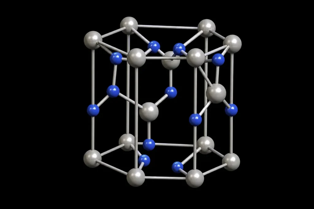
GaN crystal structure is hexagonal wurtzite, a stacking of gallium and nitrogen atoms in which each atom bonds to four neighbours of the other kind. At 300 K the lattice constants are a ≈ 3.189 Å and c ≈ 5.185 Å. The structure lacks inversion symmetry, which gives GaN its polarity and built-in polarization.
Key takeaways
- Wurtzite (space group P63mc) is the stable phase of GaN at normal temperature and pressure.
- Lattice constants: a ≈ 3.189 Å, c ≈ 5.185 Å, c/a ≈ 1.626, close to the ideal 1.633.
- Ga-polar and N-polar GaN are the same crystal pointing in opposite directions along the c-axis. Most commercial MOCVD GaN is Ga-polar.
- c-plane (0001) is polar. m-plane {1−100} and a-plane {11−20} are nonpolar. Semipolar planes sit in between.
- Zincblende GaN exists but is metastable. It needs cubic substrates and has had little commercial use.
What crystal structure does GaN have?
GaN crystallises in the wurtzite structure. Wurtzite is a hexagonal lattice made of two interpenetrating hexagonal close-packed sublattices, one of gallium and one of nitrogen. The sublattices are offset along the c-axis by about 0.377c, a value called the internal parameter u. Each gallium atom sits at the centre of a tetrahedron of four nitrogen atoms, and the reverse.
Along the c-axis, the atomic layers stack in an ABAB sequence of Ga–N bilayers. That stacking is the difference between wurtzite and zincblende, which stacks ABCABC. Both have tetrahedral bonding. The change in stacking alters symmetry, band structure and polarization.
Wurtzite is the thermodynamically stable phase of GaN, AlN and InN at ambient conditions. It is the form used in essentially every commercial LED, laser diode, HEMT and power transistor. For the full property set of the material, see our gallium nitride hub and the GaN properties table.
GaN lattice parameters
| Parameter (300 K) | Wurtzite GaN | Wurtzite AlN | Wurtzite InN | Zincblende GaN |
|---|---|---|---|---|
| a (Å) | 3.189 | 3.112 | 3.545 | About 4.50 (cubic) |
| c (Å) | 5.185 | 4.982 | 5.703 | Not applicable |
| c/a | About 1.626 | About 1.601 | About 1.609 | Not applicable |
| Bandgap (eV) | About 3.4, direct | About 6.0 to 6.2, direct | About 0.7, direct | About 3.2 to 3.3, direct |
| Space group | P63mc | P63mc | P63mc | F−43m |
| Stability | Stable | Stable | Stable | Metastable |
The ideal wurtzite c/a ratio for perfect tetrahedra is √(8/3) ≈ 1.633. GaN is slightly below it and AlN further below. That distortion from the ideal shape is one reason AlN has much stronger spontaneous polarization than GaN.
What is Ga-polar vs N-polar GaN?
Polarity describes which way the crystal points along its c-axis. Each Ga–N bilayer has the gallium atom on one side and the nitrogen atom on the other. Because wurtzite has no inversion symmetry, the [0001] and [000−1] directions are not equivalent.
By convention, the [0001] direction points from a gallium atom to its nitrogen neighbour along the bond parallel to the c-axis. Ga-polar GaN is grown along [0001]. N-polar GaN is grown along [000−1]. Polarity is a property of the bulk crystal orientation, not of which atom happens to be on the very top of the surface.
Polarity has practical effects:
- Growth. MOCVD on sapphire with a nucleation layer normally gives Ga-polar films. N-polar films need specific substrate treatments, miscut substrates or MBE conditions.
- Chemistry. N-polar GaN etches readily in hot KOH. Ga-polar GaN is far more resistant. Wet etching is a quick way to check polarity, and it is how LED makers roughen the N-face after laser lift-off to improve light extraction.
- Polarization sign. Flipping polarity flips the direction of the built-in polarization. In an AlGaN/GaN stack, Ga-polar growth puts the two-dimensional electron gas below the barrier; N-polar growth puts it above. N-polar HEMTs are studied for high-frequency devices for this reason.
- Impurities. Oxygen and other impurities incorporate differently on the two faces, so background doping often differs.
Our guide to GaN polarization explains how polarity sets the sign of the interface charge.
What are c-plane, m-plane and a-plane?
Hexagonal crystals use four-index Miller-Bravais indices (hkil), where i = −(h + k). The redundant third index makes symmetry-equivalent planes look alike. A bar or minus sign over an index marks a negative value; here it is written as −1.
| Plane | Indices | Orientation | Polar character | Typical use |
|---|---|---|---|---|
| c-plane | (0001) | Perpendicular to the c-axis | Polar, maximum polarization | Almost all commercial LEDs and HEMTs |
| m-plane | {1−100} | Parallel to c-axis, hexagon side faces | Nonpolar | Research LEDs and lasers without built-in fields |
| a-plane | {11−20} | Parallel to c-axis, through hexagon corners | Nonpolar | Research LEDs; grown on r-plane sapphire |
| Semipolar | e.g. (20−21), (11−22), (10−11) | Inclined to c-axis | Reduced polarization | Green laser diodes, high-indium InGaN |
The choice of plane matters most for light emitters. On c-plane, InGaN quantum wells carry strong internal electric fields that separate electrons and holes. On m-plane and a-plane, the polarization vector lies in the plane of the well and produces no field across it. Semipolar planes reduce the field and also tend to take up indium well, which is why they have been used for green laser diodes. The trade-off is cost: nonpolar and semipolar wafers are usually sliced from bulk GaN boules and are small and expensive.
Does zincblende GaN exist?
Yes. Zincblende GaN, also called cubic or β-GaN, is a metastable phase with a cubic lattice constant of about 4.50 Å and a direct bandgap of about 3.2 to 3.3 eV at 300 K. It forms when GaN is grown on cubic substrates such as GaAs (001) or 3C-SiC, usually by MBE at controlled conditions.
Zincblende GaN is interesting because its higher symmetry removes spontaneous polarization along the growth direction, and its slightly smaller gap could help green emission. In practice, it tends to contain wurtzite inclusions and stacking faults, because the energy difference between the two stackings is small. A third phase, rocksalt, appears only at very high pressure, in the tens of GPa range. Neither cubic phase is used in mainstream products today.
How crystal structure affects substrates and defects
Because large native GaN wafers are costly, most GaN is grown on foreign substrates with a different lattice and thermal expansion.
- Sapphire (0001). The GaN lattice rotates 30° in plane to fit. The remaining mismatch is about 16 %.
- 6H- or 4H-SiC (0001). Mismatch is about 3.5 %, the closest of the common options. Used for RF HEMTs.
- Si (111). The three-fold surface aligns with wurtzite’s hexagonal plane. Mismatch is about 17 %, and the thermal expansion difference causes tensile stress on cooling, so strain-management buffers are needed.
These mismatches create threading dislocations that run along the c-axis through the film. Their density and effects are covered in our article on defects in GaN. For a property-by-property view of GaN against its rivals, see the comparison tables.
Why the structure matters for devices
Three device facts follow directly from wurtzite symmetry. First, the polar c-axis creates spontaneous and piezoelectric polarization, which is what forms the high-density electron channel in AlGaN/GaN HEMTs without any intentional doping. Second, the same fields red-shift and weaken emission in c-plane InGaN quantum wells. Third, wurtzite’s direct gap across the whole AlN–GaN–InN family lets one material system span deep ultraviolet to near infrared, covered further in our piece on nitride ultraviolet LEDs.
FAQ
Is GaN hexagonal or cubic?
Stable GaN is hexagonal (wurtzite). A cubic zincblende form can be grown on cubic substrates but is metastable.
What are the lattice constants of GaN?
For wurtzite GaN at 300 K, a ≈ 3.189 Å and c ≈ 5.185 Å. Strain from the substrate shifts measured values slightly.
How do you tell Ga-polar from N-polar GaN?
The simplest test is a wet etch in hot KOH: N-polar surfaces etch and roughen, Ga-polar surfaces barely change. Convergent-beam electron diffraction and other methods give a direct structural check.
Why are most GaN devices made on c-plane?
c-plane films grow smoothly on large, low-cost sapphire, SiC and silicon wafers. Nonpolar and semipolar films mostly need small, costly bulk GaN wafers.
Sources
- Ioffe Institute, New Semiconductor Materials (NSM) archive, entries for GaN, AlN and InN.
- I. Vurgaftman and J. R. Meyer, “Band parameters for nitrogen-containing semiconductors,” Journal of Applied Physics (2003).
- O. Ambacher et al., “Two-dimensional electron gases induced by spontaneous and piezoelectric polarization charges in N- and Ga-face AlGaN/GaN heterostructures,” Journal of Applied Physics (1999).
- S. M. Sze and K. K. Ng, Physics of Semiconductor Devices, 3rd ed., Wiley.



