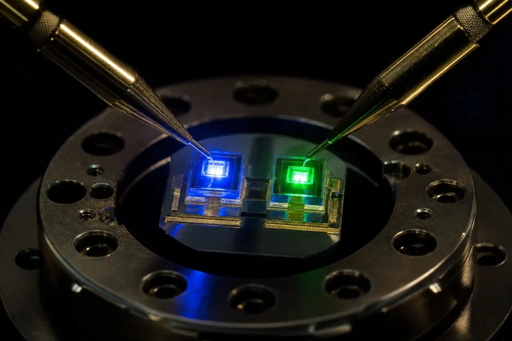
InGaN (indium gallium nitride, InxGa1−xN) is a wurtzite alloy of GaN and InN whose direct bandgap can be tuned from about 3.4 eV to about 0.7 eV by indium content. It forms the light-emitting quantum wells in blue, green and white LEDs and in violet and blue laser diodes.
Key takeaways
- End points at room temperature: GaN about 3.4 eV (365 nm), InN about 0.7 eV (about 1.8 µm). The InN value was revised down from about 1.9 eV in the early 2000s.
- Bandgap bowing is large: a widely used fit gives b ≈ 1.4 eV (Wu and co-workers, 2002).
- Blue LEDs near 450 nm use roughly 15 % to 20 % indium in the wells; green near 520 to 530 nm needs roughly 25 % to 30 %. Strain, well width and polarization shift these figures.
- InN and GaN differ by about 11 % in lattice constant. High-indium InGaN is strained, prone to phase separation and grown cool, around 700 to 800 °C.
- Efficiency falls as wavelength moves from blue to green and yellow. That drop is the green gap.
What is InGaN?
InGaN is a ternary alloy: a compound semiconductor with three elements, here indium and gallium sharing the group-III sites and nitrogen on the group-V sites. The subscript x in InxGa1−xN is the indium mole fraction. At x = 0 the crystal is GaN; at x = 1 it is InN. It has the same wurtzite structure as GaN and stays a direct-gap semiconductor across the whole range, so it emits light efficiently at every composition in principle.
InGaN is almost always used in thin layers. A typical LED active region is a stack of several InGaN quantum wells, each about 2 to 3 nm thick, separated by GaN barriers. The wells trap electrons and holes so they recombine and emit light. For the general method behind alloy tuning, see semiconductor alloys and bandgap engineering. For the host material, see our gallium nitride hub.
Bright blue InGaN LEDs arrived in the early 1990s, led by Shuji Nakamura’s work at Nichia on InGaN growth and double-heterostructure LEDs, building on p-type doping work by Amano and Akasaki. Blue InGaN chips coated with a yellow phosphor became the basis of white LED lighting.
InGaN properties by composition
The table uses Vegard’s law for lattice constant and Eg(x) = 3.4(1−x) + 0.7x − 1.4x(1−x) eV for relaxed alloy bandgap. Real quantum wells emit at somewhat longer wavelengths than relaxed bulk values because of polarization fields, and the exact numbers vary with strain.
| Indium fraction x | Relaxed a (Å) | Approx. bandgap (eV) | Approx. wavelength (nm) | Typical role |
|---|---|---|---|---|
| 0 (GaN) | 3.189 | 3.4 | 365 | Barriers, buffers |
| 0.10 | About 3.225 | About 3.0 | About 410 | Violet LEDs and laser diodes |
| 0.20 | About 3.260 | About 2.6 to 2.7 | About 460 to 470 | Blue LEDs (QW emission near 450 nm) |
| 0.30 | About 3.296 | About 2.3 | About 540 | Green LEDs |
| 0.40 | About 3.332 | About 2.0 | About 620 | Red InGaN, still in development |
| 1 (InN) | 3.545 | About 0.7 | About 1,800 | Research only |
How does indium content change emission colour?
More indium narrows the bandgap, and a narrower gap emits longer wavelengths, through λ (nm) ≈ 1240 / Eg (eV). The relationship is not linear because of bowing: the alloy gap sags below the straight line joining GaN and InN by b·x(1−x). With b ≈ 1.4 eV, the sag at x = 0.3 is about 0.3 eV. Without bowing, green would need more indium than it does.
Three other factors move the colour in real devices.
- Strain. InGaN wells are compressed to the GaN lattice. Compression slightly widens the gap compared with relaxed material.
- Quantum confinement. Thin wells raise the electron and hole levels above the band edges, shifting emission to shorter wavelengths.
- Polarization. On c-plane, the strain-induced piezoelectric field across the well tilts the bands and red-shifts emission. This is the quantum-confined Stark effect, explained in our GaN polarization guide. It also makes green LEDs blue-shift as current rises.
What is the green gap?
The green gap is the dip in LED efficiency between roughly 530 nm and 590 nm. Blue InGaN LEDs and red-to-amber AlGaInP LEDs both reach high efficiency. Between them, neither material family performs as well. InGaN loses efficiency as indium rises toward green and yellow. AlGaInP loses efficiency as it is pushed toward green, because its gap turns indirect.
For InGaN, the causes overlap:
- Stronger polarization fields at higher indium reduce electron-hole overlap and the radiative rate.
- Lower growth temperature, needed to keep indium in the film, gives poorer crystal quality and more point defects.
- More strain generates defects such as V-pits and misfit dislocations at high indium.
- Composition inhomogeneity broadens the emission and can create non-radiative regions.
A related problem is efficiency droop: the fall in efficiency of InGaN LEDs as current density rises. Auger recombination, as argued by Shen and co-workers in Applied Physics Letters (2007), and electron leakage over the active region are the leading explanations. Droop is worse in green LEDs. Commercial white LEDs sidestep the green gap by converting blue light with phosphors instead of emitting green directly.
Why is high-indium InGaN hard to grow?
Four physical limits stack up.
- Weak In–N bond. InN decomposes at much lower temperature than GaN, and indium desorbs from the growth surface. InGaN wells are therefore grown at about 700 to 800 °C, compared with about 1,000 to 1,100 °C for GaN. Lower temperature means less mobile adatoms and more defects.
- Lattice mismatch. InN’s a-lattice constant (3.545 Å) is about 11 % larger than GaN’s (3.189 Å). A 30 % indium well on GaN is under roughly 3 % compressive strain, which limits how thick it can grow before relaxing through defects.
- Phase separation. InGaN has a large miscibility gap, a composition range where a uniform alloy is thermodynamically unstable and tends to split into indium-rich and indium-poor regions. Ho and Stringfellow calculated in Applied Physics Letters (1996) that equilibrium solubility of InN in GaN at typical growth temperatures is only a few percent. Practical InGaN with 20 % to 30 % indium exists because growth is far from equilibrium and strain partly suppresses separation.
- Composition pulling. Strain makes it harder to incorporate indium into a layer matched to GaN, so indium content can rise with thickness and vary across the wafer.
Mild indium fluctuations are not all bad. They form local potential minima that trap carriers away from threading dislocations, which is one reason InGaN LEDs work on defective GaN-on-sapphire. Our article on defects in GaN covers that effect.
Approaches to longer wavelengths
- Semipolar and nonpolar substrates reduce the polarization field and, on some planes, take up indium more easily. They have been used for green laser diodes.
- Strain relaxation using relaxed InGaN templates or porous GaN lets more indium in at a given temperature.
- Barrier and interlayer design, such as AlGaN interlayers, protects wells during heating and limits indium loss.
- Red InGaN is being pursued for micro-LED displays, where using one material for red, green and blue would simplify assembly. Efficiencies remain well below AlGaInP red.
On the short-wavelength side, InGaN is paired with or replaced by AlGaN. See our piece on nitride ultraviolet LEDs. For side-by-side data on emitter materials, see the comparison tables.
FAQ
What is the bandgap of InGaN?
It ranges from about 3.4 eV (GaN) to about 0.7 eV (InN) depending on indium content, with large bowing. Blue LED wells sit near 2.7 to 2.8 eV of emitted photon energy.
Why is InN’s bandgap quoted differently in old papers?
Early InN films were polycrystalline and heavily doped, which gave an apparent gap near 1.9 eV. Better MBE-grown films in the early 2000s showed the true gap is about 0.7 eV.
Is InGaN used in solar cells?
It has been studied because its gap range covers most of the solar spectrum, but phase separation and poor p-type doping at high indium have kept it in research.
How do white LEDs use InGaN?
Most white LEDs use a blue InGaN chip near 450 nm with a yellow-emitting phosphor, often cerium-doped YAG. The mix appears white.
Sources
- J. Wu et al., “Small band gap bowing in In1−xGaxN alloys,” Applied Physics Letters (2002).
- I-hsiu Ho and G. B. Stringfellow, “Solid phase immiscibility in GaInN,” Applied Physics Letters (1996).
- Y. C. Shen et al., “Auger recombination in InGaN measured by photoluminescence,” Applied Physics Letters (2007).
- S. Nakamura and co-workers, work on InGaN growth and high-brightness InGaN blue LEDs at Nichia in the early 1990s.
- I. Vurgaftman and J. R. Meyer, “Band parameters for nitrogen-containing semiconductors,” Journal of Applied Physics (2003); Ioffe Institute NSM archive, GaN and InN entries.



