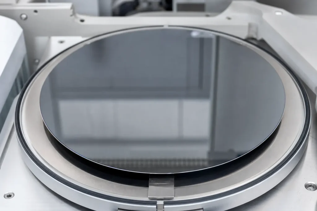
GaAs wafers are single-crystal gallium arsenide substrates, sold mainly in 100 mm and 150 mm diameters. They come in two classes. Semi-insulating wafers, with resistivity above about 107 Ω·cm, carry RF transistors and MMICs. Conductive n-type or p-type wafers carry LEDs and lasers. Most are now grown by vertical gradient freeze (VGF) rather than LEC.
Key takeaways
- Common diameters: 50 mm, 75 mm, 100 mm and 150 mm. 150 mm is the standard for RF device fabs; smaller sizes remain common in optoelectronics and R&D.
- Semi-insulating (SI) GaAs relies on a deep donor called EL2, about 0.75 eV below the conduction band, to pin the Fermi level near mid-gap.
- Conductive wafers are usually silicon-doped n-type at roughly 1017 to 1018 cm−3, or zinc-doped p-type.
- VGF grows crystals in a low thermal gradient and gives lower dislocation density than LEC. LEC was the historical workhorse for SI wafers.
- GaAs is brittle and conducts heat at about 55 W/m·K, less than half of silicon. Both shape how wafers are handled and thinned.
What sizes are GaAs wafers?
Across the public catalogues of the main substrate suppliers as of 2025, GaAs wafers are offered in 2-inch (50 mm), 3-inch (75 mm), 4-inch (100 mm) and 6-inch (150 mm) diameters. 150 mm is the production standard for RF fabs making HBTs and pHEMTs for handsets and infrastructure. LED, laser and VCSEL lines use 100 mm and 150 mm, while 50 mm and 75 mm wafers still serve research, specialty lasers and some detector work. Check supplier datasheets for the current range, since these catalogues change.
Thickness scales with diameter to keep the wafer handleable. Typical values are about 350 µm for 50 mm wafers and about 625 µm to 675 µm for 100 mm and 150 mm wafers. Specifications vary by supplier and customer. Surface orientation is usually (100). Conductive wafers for optoelectronics are often cut a few degrees off (100) to improve epitaxial step flow, while SI wafers for transistors are usually on-axis or slightly miscut.
Compared with other substrates, GaAs sits in the middle. Silicon runs at 300 mm. SiC is at 150 mm with 200 mm ramping, as covered in our guide to SiC wafers. InP is mostly 75 mm to 100 mm.
GaAs substrate properties at 300 K
| Property (300 K) | Value | Why it matters for wafers |
|---|---|---|
| Crystal structure | Zinc blende | Cleaves along {110} planes, used to form laser facets |
| Lattice constant | 5.653 Å | Nearly matched to AlAs, so AlGaAs grows without strain |
| Bandgap | 1.424 eV, direct | Sets emission near 870 nm; allows high intrinsic resistivity |
| Intrinsic carrier concentration | About 2.1 × 106 cm−3 | Low enough for semi-insulating behaviour |
| Intrinsic resistivity | About 3.3 × 10⁸ Ω·cm | Upper bound for SI wafers |
| Electron mobility | Up to about 8,500 cm²/V·s | Basis of GaAs RF performance |
| Thermal conductivity | About 55 W/m·K | Wafers are thinned to about 100 µm for RF heat removal |
| Static dielectric constant | 12.9 | Sets microstrip line dimensions on MMICs |
| Density | 5.32 g/cm³ | Heavier and more fragile than Si |
| Melting point | About 1,238 °C | Arsenic vapour pressure at the melt drives crystal-growth design |
| Thermal expansion | About 5.7 × 10⁻⁶ /K | Mismatch with Si complicates GaAs-on-Si |
For the full electrical and optical data set, see the properties of gallium arsenide.
What is semi-insulating GaAs?
Semi-insulating GaAs is a substrate with resistivity high enough, typically 107 Ω·cm or more, that it behaves almost like an insulator. It is not a true insulator. It is a semiconductor whose free-carrier concentration has been pushed close to the intrinsic level.
That matters because RF circuits need a substrate that does not leak current or absorb signal. On an SI GaAs wafer, transistors, inductors, capacitors and transmission lines sit side by side with little loss between them. That is what makes a monolithic microwave integrated circuit (MMIC) possible. Standard silicon wafers, at a few to tens of Ω·cm, are too conductive for low-loss microwave passives unless special high-resistivity silicon is used.
Pure GaAs would be semi-insulating on its own, because its 1.42 eV bandgap gives a very low intrinsic carrier density. Real crystals are never pure. Residual carbon acts as a shallow acceptor, and silicon or other impurities act as shallow donors. Without compensation, these would make the crystal p-type or n-type. The fix is to add a deep level that soaks up those shallow carriers.
Two approaches have been used. Early SI GaAs was chromium-doped: Cr acts as a deep acceptor. Modern SI GaAs is usually undoped or lightly carbon-doped, with compensation provided by the native EL2 defect. Carbon control has become a key part of the recipe, because the balance of carbon acceptors against EL2 donors sets the final resistivity.
What is the EL2 defect?
EL2 is a deep donor level in GaAs, about 0.75 eV below the conduction band, close to mid-gap. The name comes from a 1977 survey of electron traps by Martin, Mitonneau and Mircea, where it was the second trap in their list. It is generally attributed to the arsenic antisite, an arsenic atom sitting on a gallium site, possibly in a complex with other defects. It forms naturally in arsenic-rich melt-grown crystals at concentrations of roughly 1016 cm−3.
Its job in SI wafers is compensation. EL2 donors give up electrons to shallow carbon acceptors until the acceptors are filled. The remaining EL2 levels then pin the Fermi level near mid-gap. Free-carrier density falls to near-intrinsic levels and resistivity climbs above 107 Ω·cm.
EL2 also has quirks. It is metastable: at low temperature, illumination can switch it into an inactive state, an effect called photoquenching. Its density can vary across a wafer, which once caused threshold-voltage scatter in GaAs MESFETs. Post-growth wafer annealing is widely used to make EL2 and resistivity more uniform.
Semi-insulating vs conductive GaAs
| Feature | Semi-insulating | Conductive n-type | Conductive p-type |
|---|---|---|---|
| Dopant | Undoped or C, compensated by EL2 (historically Cr) | Si (sometimes Te) | Zn |
| Resistivity or carrier density | Above about 107 Ω·cm | Roughly 1017 to 1018 cm−3 | Roughly 1018 to 1019 cm−3 |
| Main devices | HBTs, pHEMTs, MMICs, switches | LEDs, edge-emitting lasers, VCSELs, solar cells | Some laser and detector structures |
| Key quality metric | Resistivity uniformity, EL2 and carbon control | Low dislocation density for optical lifetime | Low dislocation density |
Conductive wafers need a low dislocation density more than SI wafers do. Dislocations act as non-radiative recombination centres, and in lasers they can seed dark-line defects that kill the device. Silicon doping also helps here: it hardens the lattice and reduces dislocation formation during growth.
How are GaAs crystals grown? VGF vs LEC
GaAs is harder to grow than silicon. At its melting point, about 1,238 °C, arsenic has a high vapour pressure and would boil off the melt. Both main methods control that loss, in different ways.
Liquid encapsulated Czochralski (LEC) pulls a crystal upward from a melt, as in silicon Czochralski growth. A layer of molten boron oxide (B2O3) floats on the GaAs melt and seals in the arsenic, and the chamber runs under high inert-gas pressure. LEC is fast and gives round boules. Its weakness is the steep temperature gradient near the growth interface, which creates thermal stress and dislocations.
Vertical gradient freeze (VGF) holds the melt in a crucible, usually pyrolytic boron nitride, with a seed crystal at the bottom. The furnace profile is moved slowly so the melt freezes from the seed upward. There is no pulling and the thermal gradient is much gentler. The closely related vertical Bridgman (VB) method moves the crucible instead of the profile.
| Factor | LEC | VGF / VB |
|---|---|---|
| Growth geometry | Crystal pulled from melt | Melt frozen in a crucible from the seed up |
| Thermal gradient | Steep | Low |
| Typical dislocation density (EPD) | Roughly 104 to 105 cm−2 | Roughly 102 to 104 cm−2 |
| Residual stress | Higher | Lower, fewer wafer breakages |
| Diameter control | Set by pulling; needs grinding | Set by crucible |
| Main use today | Some SI substrates, legacy lines | Most SI and conductive substrates |
The industry has largely moved to VGF and VB, especially at 150 mm, where LEC’s thermal stress gets worse with diameter. For background on how GaAs is used once the wafer exists, see understanding gallium arsenide and the GaAs materials hub. For GaAs against other substrates, see the comparisons hub.
FAQ
Why are GaAs wafers more fragile than silicon?
GaAs has lower fracture toughness and cleaves easily along {110} planes. Wafers need careful handling, especially after thinning for RF backside processing.
What resistivity counts as semi-insulating?
Typically 107 Ω·cm or higher. The intrinsic limit at 300 K is about 3.3 × 10⁸ Ω·cm.
Why are GaAs RF wafers thinned?
GaAs conducts heat at about 55 W/m·K. Thinning the wafer, often to around 100 µm, shortens the heat path to the package and allows through-wafer vias for grounding.
Is GaAs toxic to handle?
Solid GaAs wafers are stable, but grinding, polishing and dicing produce arsenic-bearing dust and slurry. Fabs treat these as hazardous waste.
Sources
- Ioffe Institute, New Semiconductor Materials (NSM) archive, gallium arsenide: basic, electrical, thermal and optical parameters.
- J. S. Blakemore, “Semiconducting and other major properties of gallium arsenide,” Journal of Applied Physics (1982).
- G. M. Martin, A. Mitonneau and A. Mircea, survey of electron traps in bulk and epitaxial GaAs crystals, Electronics Letters (1977). Origin of the EL2 label.
- S. M. Sze and K. K. Ng, Physics of Semiconductor Devices, 3rd ed., Wiley.



