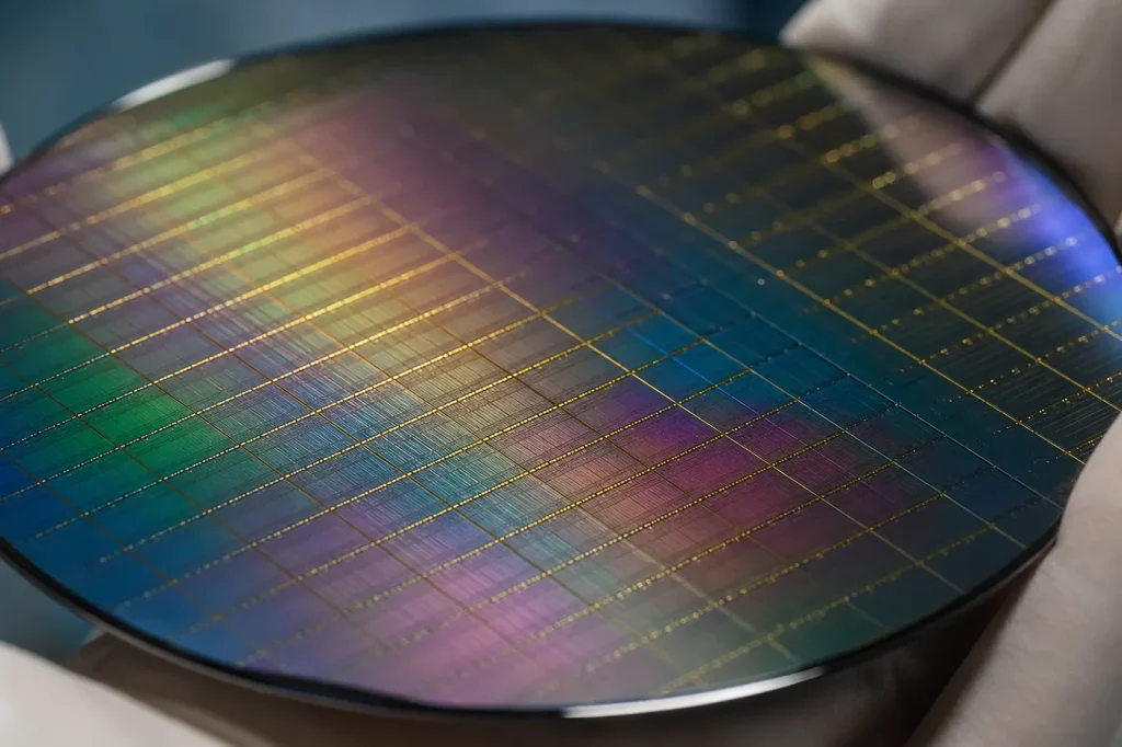
Gallium nitride (GaN) is a III-V wide-bandgap semiconductor with a direct bandgap of 3.39 eV at 300 K in its wurtzite form. Its key properties are a critical field of about 3.3 MV/cm, bulk electron mobility up to about 1,000 cm²/V·s and thermal conductivity of about 130 to 230 W/m·K (Ioffe NSM archive).
Key takeaways
- Bandgap: 3.39 eV at 300 K, direct, wurtzite GaN. About 3.47 eV near 0 K.
- Electron mobility: up to about 1,000 cm²/V·s in bulk; about 1,500 to 2,000 cm²/V·s in an AlGaN/GaN 2DEG.
- Critical field: about 3.3 MV/cm is the common design value, roughly 10x silicon.
- Thermal conductivity: about 130 W/m·K for typical material, up to about 230 W/m·K for high-quality bulk crystals.
- Lattice constants: a = 3.189 Å, c = 5.185 Å.
GaN properties table (wurtzite, 300 K)
All values are for wurtzite GaN, the stable hexagonal form used in almost every commercial device, at 300 K. Where published values differ by method or crystal quality, the table gives a range.
| Property | Value (300 K) | Unit | Source / note |
|---|---|---|---|
| Crystal structure | Wurtzite (hexagonal, P63mc) | n/a | Ioffe NSM |
| Bandgap | 3.39 (direct) | eV | Ioffe NSM; often rounded to 3.4 |
| Bandgap near 0 K | About 3.47 | eV | Ioffe NSM |
| Lattice constant a | 3.189 | Å | Ioffe NSM (reported 3.186 to 3.189) |
| Lattice constant c | 5.185 | Å | Ioffe NSM |
| Density | 6.15 | g/cm³ | Ioffe NSM |
| Electron mobility (bulk) | Up to about 1,000 | cm²/V·s | Ioffe NSM; lower in doped or defective layers |
| Electron mobility (AlGaN/GaN 2DEG) | About 1,500 to 2,000 | cm²/V·s | Widely reported in HEMT literature (Mishra et al., Proc. IEEE 2002) |
| Hole mobility (bulk) | Up to about 200; typically tens in Mg-doped p-GaN | cm²/V·s | Ioffe NSM |
| Electron saturation velocity | About 2.5 × 10⁷ | cm/s | Ioffe NSM |
| Critical (breakdown) field | About 3.3 (reported 3 to 5) | MV/cm | Common design value; depends on doping and method |
| Thermal conductivity | About 130 to 230 | W/m·K | Ioffe NSM lists about 130; high-quality bulk GaN reaches about 230 |
| Static dielectric constant | 8.9 | n/a | Ioffe NSM |
| High-frequency dielectric constant | 5.35 | n/a | Ioffe NSM |
| Electron effective mass | 0.20 | m0 | Ioffe NSM |
| Electron affinity | About 4.1 | eV | Ioffe NSM |
| Thermal expansion, a-axis | About 5.6 × 10⁻⁶ | K-1 | Ioffe NSM |
| Thermal expansion, c-axis | About 3.2 × 10⁻⁶ | K-1 | Ioffe NSM |
What is the bandgap of GaN?
Wurtzite GaN has a direct bandgap of 3.39 eV at 300 K. That corresponds to a band-edge wavelength of about 365 nm, in the near ultraviolet. The gap shrinks as temperature rises. The Ioffe archive gives a Varshni-type fit starting from about 3.47 eV near 0 K, which lands at about 3.39 eV at room temperature.
The less common zinc blende (cubic) form of GaN has a smaller gap, about 3.2 eV. It is mostly a research material. Alloying moves the gap in both directions: adding indium (InGaN) lowers it toward InN’s roughly 0.7 eV for blue and green LEDs, while adding aluminium (AlGaN) raises it toward AlN’s roughly 6.2 eV for UV emitters and transistor barriers. Our article on nitride-based UV LEDs covers the high-Al end.
What is GaN electron mobility?
The answer depends on where the electrons are. Bulk GaN has electron mobility up to about 1,000 cm²/V·s at 300 K in pure, lightly doped crystals. Typical epitaxial layers with doping and dislocations measure lower, often several hundred cm²/V·s. Silicon, for comparison, is about 1,400 cm²/V·s.
Holes are much slower. p-type GaN is doped with magnesium, which has a deep acceptor level, so only a small fraction of the dopant is ionised at room temperature. Practical p-GaN layers show hole mobility in the tens of cm²/V·s. This weak p-type performance is one reason GaN power devices are built as n-channel lateral transistors.
How do bulk and 2DEG mobility differ?
A two-dimensional electron gas (2DEG) is a thin sheet of electrons confined at the interface between two materials. In GaN devices it forms where a thin AlGaN barrier sits on top of GaN. Wurtzite nitrides have strong built-in spontaneous and piezoelectric polarisation. The mismatch in polarisation between AlGaN and GaN leaves a fixed positive charge at the interface, and electrons gather there to balance it. No intentional doping is needed. Ambacher and co-workers laid out this mechanism in a 1999 Journal of Applied Physics paper that is still the standard reference.
Two things make 2DEG mobility higher than bulk mobility:
- No dopant atoms in the channel. In bulk material, ionised donors scatter electrons. In a 2DEG the charge comes from polarisation, so the channel stays undoped.
- Confinement. Electrons move in a plane, which changes how they scatter and supports high sheet density.
Typical room-temperature values are about 1,500 to 2,000 cm²/V·s with sheet carrier densities around 1013 cm-2. That combination gives low channel resistance and is the basis of the GaN high-electron-mobility transistor (HEMT). When a datasheet or press release quotes “2,000 cm²/V·s” for GaN, it means the 2DEG, not the bulk crystal.
What is GaN’s critical electric field?
The critical field is the field at which avalanche breakdown begins. For GaN the most commonly used design value is about 3.3 MV/cm. Published values range from about 3 MV/cm to about 5 MV/cm, depending on doping, crystal quality and whether the number is measured or calculated. Silicon is about 0.3 MV/cm, so GaN holds roughly ten times the field.
In real lateral HEMTs, the practical breakdown is usually set by the device design, not the material limit. Field crowding at the gate edge, buffer leakage and the silicon substrate underneath all cap the voltage first. That is why most commercial GaN power transistors are rated at 650 V or below even though the material could support more. Our breakdown field comparison lists GaN against SiC, Ga2O3 and diamond.
What is GaN thermal conductivity?
The Ioffe archive lists about 1.3 W/cm·K, or 130 W/m·K, at 300 K. High-quality bulk GaN crystals with low dislocation and impurity density have been measured at roughly 200 to 230 W/m·K. Thin epitaxial films on foreign substrates usually fall at the lower end because defects and boundaries scatter phonons.
GaN conducts heat about as well as silicon and about a third to a half as well as 4H-SiC. In high-power RF parts, heat must leave through the substrate, so the substrate choice often matters more than GaN’s own value. That is the main reason RF GaN is built on SiC. See GaN-on-Si vs GaN-on-SiC for the substrate trade-offs.
GaN compared with Si, GaAs and 4H-SiC
| Property (300 K) | Si | GaAs | 4H-SiC | GaN |
|---|---|---|---|---|
| Bandgap (eV) | 1.12 | 1.424 | 3.23 to 3.26 | 3.39 |
| Critical field (MV/cm) | About 0.3 | About 0.4 | About 2.5 to 3 | About 3.3 |
| Electron mobility (cm²/V·s) | About 1,400 | Up to 8,500 | About 900 to 1,000 | Up to 1,000 bulk; 1,500 to 2,000 2DEG |
| Saturation velocity (107 cm/s) | About 1.0 | About 0.7 to 1.0 | About 2.0 | About 2.5 |
| Thermal conductivity (W/m·K) | About 130 to 150 | About 46 to 55 | About 330 to 490 | About 130 to 230 |
The pattern: GaN matches SiC on bandgap and critical field, beats it on saturation velocity and 2DEG mobility, and loses on thermal conductivity. That is why GaN wins where switching speed and frequency matter, and SiC wins where heat and very high voltage dominate. Our full GaN vs SiC comparison turns these numbers into design guidance, and the semiconductor properties table puts GaN in context with other materials.
How to read GaN data correctly
- Check the polytype. Wurtzite and zinc blende values differ. Assume wurtzite unless stated.
- Check bulk vs 2DEG. A mobility above about 1,200 cm²/V·s almost always refers to a 2DEG.
- Check the crystal. GaN grown on Si or sapphire carries dislocation densities in the 108 to 109 cm-2 range, which lowers mobility and thermal conductivity compared with bulk GaN.
- Check direction. Thermal expansion and some optical constants differ between the a-axis and c-axis.
FAQ
Is GaN a direct bandgap semiconductor?
Yes. Wurtzite GaN has a direct gap of 3.39 eV at 300 K. That makes it an efficient light emitter and the base of blue LEDs and laser diodes.
What is the melting behaviour of GaN?
GaN does not melt cleanly at atmospheric pressure. It decomposes into gallium and nitrogen first. That is why GaN crystals cannot be pulled from a melt like silicon, and why native GaN wafers are small and expensive.
What is the dielectric constant of GaN?
The static dielectric constant of wurtzite GaN is about 8.9 and the high-frequency value is about 5.35, per the Ioffe archive.
Why is GaN used in power electronics?
Its roughly 10x higher critical field than silicon allows thinner, smaller devices for the same voltage, and its 2DEG gives low on-resistance and fast switching. Our overview of GaN for high-power applications covers the device side.
Sources
- Ioffe Institute, New Semiconductor Materials (NSM) archive, GaN section: http://www.ioffe.ru/SVA/NSM/Semicond/
- U. K. Mishra, P. Parikh and Y.-F. Wu, “AlGaN/GaN HEMTs: an overview of device operation and applications,” Proceedings of the IEEE (2002).
- O. Ambacher et al., “Two-dimensional electron gases induced by spontaneous and piezoelectric polarization charges in N- and Ga-face AlGaN/GaN heterostructures,” Journal of Applied Physics (1999).
- I. Vurgaftman, J. R. Meyer and L. R. Ram-Mohan, “Band parameters for III-V compound semiconductors and their alloys,” Journal of Applied Physics (2001).
- T. Kimoto and J. A. Cooper, Fundamentals of Silicon Carbide Technology, Wiley-IEEE Press.



