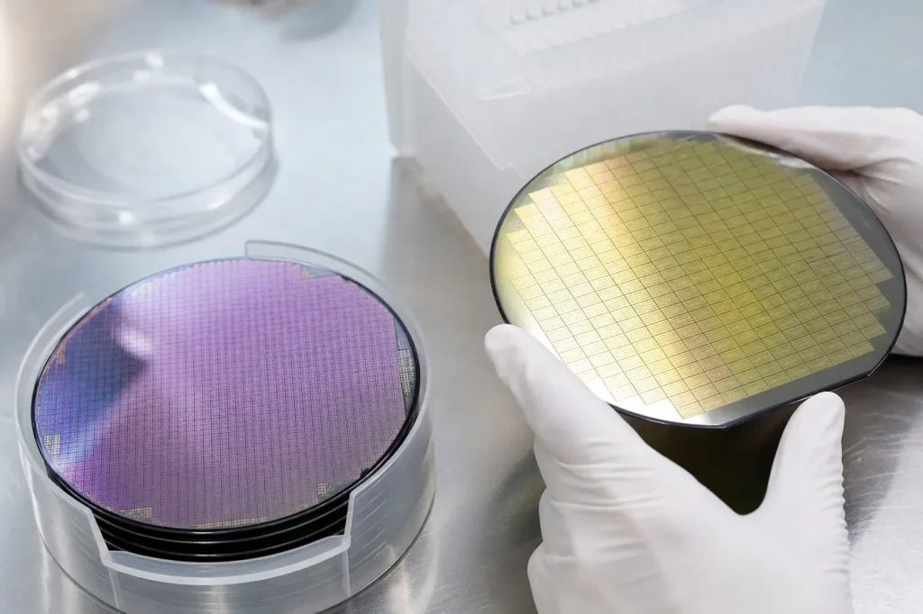
III-V semiconductors are compound semiconductors made by bonding an element from group 13 of the periodic table (boron, aluminium, gallium, indium) with one from group 15 (nitrogen, phosphorus, arsenic, antimony). Most have a direct bandgap and high electron mobility, which is why they dominate lasers, LEDs, RF amplifiers and fast photodetectors.
Key takeaways
- A III-V is one group 13 element plus one group 15 element. GaAs, InP, GaN and AlN are the commercial workhorses.
- Bandgaps at 300 K span from 0.17 eV (InSb) to about 6.2 eV (AlN), so the family covers the infrared through the deep ultraviolet.
- Most III-Vs have a direct gap. GaP and AlAs are the main indirect exceptions.
- Alloys such as InGaAsP and InGaN let engineers tune the bandgap, and with it the emission wavelength.
- AlN has the widest bandgap of the common III-V binaries.
What is a III-V semiconductor?
The name comes from the old periodic-table numbering. Group III (now group 13) elements have three valence electrons. Group V (now group 15) elements have five. Pair one atom of each and the crystal averages four valence electrons per atom, the same as silicon. That count lets the atoms form the same tetrahedral covalent bonds that make silicon a semiconductor.
The difference is that the bond is partly ionic. The group 15 atom pulls electron density toward itself. That changes the band structure, and in most III-Vs it moves the lowest point of the conduction band directly above the highest point of the valence band. This is called a direct bandgap. It is the single most important property of the family, and we come back to it below.
III-Vs are one branch of the wider class of compound semiconductors. Other branches include the II-VI compounds (CdTe, ZnSe) and the group IV compound silicon carbide (SiC). If you are new to the topic, our primer on the basics of compound semiconductors covers bonding and doping in more depth.
Which elements form III-V compounds?
The group 13 side contributes boron (B), aluminium (Al), gallium (Ga) and indium (In). Thallium is in the group but is rarely used. The group 15 side contributes nitrogen (N), phosphorus (P), arsenic (As) and antimony (Sb). Bismuth appears only in small amounts in research alloys.
Combining these gives two structural families:
- Nitrides (GaN, AlN, InN) normally crystallise in the hexagonal wurtzite structure. They have short, strong bonds and wide bandgaps.
- Phosphides, arsenides and antimonides (GaAs, InP, GaP, InAs, GaSb, InSb, AlAs) crystallise in the cubic zinc blende structure. Their bandgaps run from the infrared to the visible.
Mixing three or four elements gives ternary and quaternary alloys: AlGaAs, InGaAs, InGaAsP, AlGaN, InGaN. The bandgap and the lattice constant both shift with composition. Engineers pick a composition that hits the target wavelength and still matches the lattice of an available substrate. Lattice matching matters because a mismatched layer relaxes by forming dislocations, and dislocations kill light emission.
III-V binaries compared: bandgap, gap type and mobility
The table lists the main binary compounds. Values are at 300 K and come from the Ioffe Institute NSM archive unless noted. Mobility figures are upper bounds for pure, lightly doped bulk material. Real device layers are usually lower.
| Material | Crystal structure | Bandgap (eV, 300 K) | Gap type | Electron mobility (cm²/V·s, 300 K) | Typical uses |
|---|---|---|---|---|---|
| AlN | Wurtzite | 6.0 to 6.2 | Direct | About 300 | Deep-UV LEDs, piezoelectric filters, thermal substrates |
| GaN | Wurtzite | 3.39 | Direct | Up to 1,000 (bulk) | Blue and white LEDs, lasers, power and RF HEMTs |
| GaP | Zinc blende | 2.26 | Indirect | Up to 250 | Green and yellow indicator LEDs |
| AlAs | Zinc blende | 2.12 to 2.16 | Indirect | Low; rarely used as a channel | Barrier layers and Bragg mirrors in GaAs stacks |
| GaAs | Zinc blende | 1.424 | Direct | Up to 8,500 | RF front-ends, 850 nm VCSELs, solar cells |
| InP | Zinc blende | 1.344 | Direct | Up to 5,400 | Telecom lasers and photodiodes, high-speed transistors |
| GaSb | Zinc blende | 0.726 | Direct | Up to 3,000 | Mid-infrared lasers and detectors |
| InN | Wurtzite | About 0.7 | Direct | Reported values vary widely | Indium source in InGaN alloys |
| InAs | Zinc blende | 0.354 | Direct | Up to 40,000 | Infrared detectors, Hall sensors |
| InSb | Zinc blende | 0.17 | Direct | Up to 77,000 | Mid-infrared imaging, magnetic sensors |
Two patterns stand out. First, bandgap rises as the atoms get lighter and the bonds get shorter: InSb is at the bottom, AlN at the top. Second, electron mobility moves the other way. The narrow-gap indium compounds have very light electrons and mobilities tens of times higher than silicon (about 1,400 cm²/V·s). For a side-by-side view including silicon, germanium and SiC, see our semiconductor properties table.
Direct vs indirect bandgap: why it matters
In a direct-gap material, an electron at the bottom of the conduction band can drop into a hole at the top of the valence band and release its energy as a photon. Momentum is already matched, so nothing else is needed.
In an indirect-gap material such as silicon, GaP or AlAs, the two band edges sit at different crystal momenta. A photon carries almost no momentum, so the transition also needs a phonon (a lattice vibration). That three-body event is far less likely. Most of the energy is lost as heat instead of light. This is the basic reason silicon is a poor light emitter and why the photonics industry runs on III-Vs.
GaP is the useful exception. Doping it with nitrogen creates states that allow reasonably efficient green emission, which is why GaP indicator LEDs were common for decades. They are now largely replaced by InGaN and AlGaInP devices that emit far more light per watt.
Why are III-V semiconductors used for lasers?
A laser needs population inversion and efficient stimulated emission. Both depend on electrons recombining radiatively, which requires a direct gap. III-Vs add three more advantages.
- Tunable wavelength. The photon energy is set by the bandgap. Alloying lets designers dial it in. InGaAsP on InP covers the 1.3 µm and 1.55 µm telecom windows, where optical fibre has its lowest dispersion and loss. AlGaAs on GaAs covers the 780 to 870 nm range used in VCSELs for data links and sensing.
- Heterostructures. Lattice-matched pairs such as AlGaAs/GaAs and InGaAsP/InP can be grown in layers a few nanometres thick. A narrow-gap quantum well between wider-gap barriers traps both electrons and light, which lowers the threshold current.
- Short wavelengths from nitrides. InGaN quantum wells on GaN produce violet and blue light. Blue InGaN laser diodes at about 405 nm made Blu-ray possible. The 2014 Nobel Prize in Physics went to Akasaki, Amano and Nakamura for efficient blue LEDs built on this material system.
The same logic applies to photodetectors. InGaAs lattice-matched to InP absorbs strongly out to about 1.7 µm, so it is the standard detector material for fibre receivers and short-wave infrared cameras.
Which III-V has the widest bandgap?
Among the common binaries, aluminium nitride (AlN) has the widest bandgap, at about 6.0 to 6.2 eV at 300 K. That corresponds to an emission wavelength near 200 to 210 nm, deep in the ultraviolet. AlGaN alloys bridge the range between GaN (3.39 eV, about 365 nm) and AlN, which is how deep-UV LEDs for disinfection and sensing are made. Our article on nitride UV LEDs covers the efficiency problems that still limit them.
Boron nitride is sometimes listed as a III-V too. Its cubic and hexagonal forms have gaps in the same broad range as AlN, but reported values differ between studies and doping it for devices remains difficult, so it is mostly a research material today.
Wide-gap nitrides also matter for electronics, not just light. A wider gap supports a higher breakdown field, which is why GaN transistors can block hundreds of volts in a small area. We cover that link in our guide to wide-bandgap semiconductors.
Where III-Vs are used, by material
- GaAs: power amplifiers and switches in phone front-ends, 850 nm and 940 nm VCSELs, and high-efficiency multi-junction solar cells for satellites.
- InP: lasers, modulators and photodiodes for fibre networks and data centres, plus very high-frequency transistors.
- GaN: blue and white LEDs, laser diodes, power transistors from roughly 100 V to 650 V, and RF amplifiers for radar and base stations. See our GaN properties table for the full data set.
- AlN and AlGaN: deep-UV emitters, the barrier layer in GaN transistors, and piezoelectric RF filters.
- InAs, InSb, GaSb: infrared detectors, thermal imaging and magnetic field sensors.
The trade-offs: why III-Vs have not replaced silicon
III-Vs beat silicon on light emission and, in many cases, on electron mobility. Silicon still wins on almost everything that matters for logic and memory.
- No good native oxide. Silicon grows SiO2, an excellent insulator with a clean interface. III-Vs do not, which makes MOS transistors much harder to build.
- Smaller, costlier wafers. Silicon is processed on 300 mm wafers. GaAs and InP substrates are typically 100 mm to 150 mm and cost far more per unit area.
- Poor hole mobility. Most III-Vs conduct holes much worse than electrons, which hurts complementary (CMOS-style) circuits.
- Toxic precursors. Arsenic and phosphorus sources such as arsine and phosphine need strict handling in the fab.
The practical result is a division of labour. Silicon handles computation. III-Vs handle light, high frequency and, increasingly, high-voltage power conversion where GaN competes with silicon and SiC.
FAQ
Is silicon carbide a III-V semiconductor?
No. SiC combines two group 14 elements, silicon and carbon, so it is a IV-IV compound. It is a compound semiconductor and a wide-bandgap one (about 3.26 eV for 4H-SiC at 300 K), but not a III-V.
Is GaAs a direct or indirect bandgap semiconductor?
GaAs has a direct bandgap of 1.424 eV at 300 K. That is why it emits efficiently in the near infrared, around 870 nm for the pure binary.
Which III-V has the highest electron mobility?
InSb, with bulk electron mobility up to about 77,000 cm²/V·s at 300 K according to the Ioffe archive. InAs follows at up to about 40,000 cm²/V·s. Both have narrow gaps, so they are used mainly in sensors and infrared devices rather than power electronics.
Why do III-V lasers need lattice-matched substrates?
If the layer and substrate lattice constants differ, the strain relaxes by forming dislocations. Dislocations act as non-radiative recombination centres and shorten laser life. Matching InGaAsP to InP, or AlGaAs to GaAs, keeps the defect density low.
Sources
- Ioffe Institute, New Semiconductor Materials (NSM) archive: http://www.ioffe.ru/SVA/NSM/Semicond/
- I. Vurgaftman, J. R. Meyer and L. R. Ram-Mohan, “Band parameters for III-V compound semiconductors and their alloys,” Journal of Applied Physics (2001).
- S. M. Sze and K. K. Ng, Physics of Semiconductor Devices, 3rd ed., Wiley.
- Nobel Prize in Physics 2014 announcement for efficient blue LEDs: https://www.nobelprize.org/



