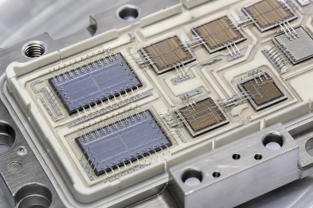
SiC MOSFET vs Si IGBT is the main power-switch choice from 650 V to 1,700 V. A silicon carbide MOSFET is a unipolar switch with no tail current, so it switches faster with lower loss. A silicon IGBT is a bipolar switch that costs less per amp. Pick SiC for high frequency and light-load efficiency, IGBT for cost.
Key takeaways
- SiC’s critical field of about 2–3 MV/cm, roughly 7–10 times silicon’s 0.3 MV/cm, lets a 1,200 V MOSFET use a drift layer of about 10 µm instead of the roughly 100 µm a silicon device needs.
- An IGBT conducts with a fixed knee voltage of about 0.7 V plus a resistive part. A SiC MOSFET behaves like a resistor, so it wins at partial load.
- IGBTs turn off with a tail current from stored charge. SiC MOSFETs have none, which cuts turn-off loss and lets them switch several times faster.
- IGBTs remain cheaper per amp, tolerate short circuits longer and dominate slow, high-current drives. SiC dominates where frequency, size or efficiency pays for the premium.
How the two devices work
An insulated-gate bipolar transistor (IGBT) is a MOS-gated device with a p+ collector under the drift region. When it turns on, the collector injects holes into the drift layer. That flood of minority carriers, called conductivity modulation, drops the drift resistance sharply. It is how a silicon device with a thick, lightly doped drift region can still conduct hundreds of amps at 1,200 V.
A SiC MOSFET is unipolar: only electrons carry current, and nothing is stored. It does not need conductivity modulation, because SiC’s high critical field allows a drift layer about one-tenth as thick and far more heavily doped. Our breakdown field comparison shows the drift-layer arithmetic.
| Attribute | Si IGBT | SiC MOSFET |
|---|---|---|
| Carrier type | Bipolar (electrons and holes) | Unipolar (electrons) |
| Material critical field (MV/cm, 300 K) | ~0.3 | ~2–3 (4H-SiC) |
| Material thermal conductivity (W/m·K) | 130–150 | ~370 |
| On-state behaviour | Knee voltage (~0.7 V) plus resistance | Resistive, no knee |
| Turn-off | Tail current from stored charge | No tail current |
| Reverse conduction | Needs anti-parallel diode | Body diode, or added SiC Schottky diode |
| Typical short-circuit withstand | ~10 µs class | A few µs, part-dependent |
| Typical gate drive | +15 V on, 0 to −15 V off | +15 to +20 V on, about −2 to −5 V off |
| Common voltage classes | 600 V to 6.5 kV | 650 V to 1,700 V mainstream; higher in development |
Conduction losses compared
Conduction loss is the power lost while the switch is on. The two devices follow different curves.
- IGBT: P ≈ VCE0·I + rCE·I2. The threshold VCE0, about 0.7 V or more, comes from the collector p-n junction and is paid even at low current. A 1,200 V IGBT at rated current typically shows a saturation voltage of roughly 1.5–2.5 V.
- SiC MOSFET: P = RDS(on)·I2. With no knee, the voltage drop shrinks in proportion to current.
The result is a crossover. At light and medium load, the SiC MOSFET has the lower drop. At very high current density, the IGBT’s conductivity modulation can catch up. SiC RDS(on) also rises with junction temperature, so compare at hot conditions, typically 150 °C or 175 °C, not only at 25 °C.
To compare real parts, take a 1,200 V SiC MOSFET and a 1,200 V IGBT with similar current ratings and package, then read VCE(sat) and RDS(on) at the same current and junction temperature from current datasheets. We deliberately do not print one pair of part numbers here, because product generations change every year or two and a single snapshot misleads.
How switching losses compare
Switching loss is energy lost in each turn-on and turn-off, multiplied by switching frequency. This is where SiC pulls ahead.
- Turn-off. When an IGBT’s gate turns off, the stored holes in the drift region must recombine. Current decays slowly in a tail while voltage is already high, and that overlap is lost energy (Eoff). A SiC MOSFET has no stored charge, so Eoff is much smaller.
- Turn-on. In a bridge, the IGBT turns on against the opposite switch’s freewheeling silicon diode, whose reverse recovery adds to Eon. SiC body diodes and SiC Schottky diodes have far lower recovery charge.
- Temperature. IGBT tail current and silicon diode recovery grow with temperature. SiC switching energy is nearly flat with temperature.
Datasheets at the same voltage and current rating generally show SiC MOSFET total switching energy several times lower than an IGBT plus silicon diode. The exact factor depends on gate resistance, stray inductance and test conditions, so compare datasheet curves taken under matching conditions.
Switching frequency range for each
| Application | Si IGBT typical range | SiC MOSFET typical range |
|---|---|---|
| Industrial motor drives | ~2–20 kHz | ~10–40 kHz |
| EV traction inverters | ~8–20 kHz | ~10–30 kHz |
| Solar inverters, DC-DC and chargers | ~15–40 kHz | ~50–200 kHz and above |
Traction inverters do not usually push SiC to very high frequency, because motor windings and EMI limits cap the benefit. There the gain is lower loss at the same frequency. In DC-DC converters and on-board chargers, higher frequency shrinks inductors and transformers, so SiC changes the whole design.
Why EV inverters are moving to SiC
- Partial-load efficiency. A car spends most of its time at a small fraction of peak power. The IGBT’s knee voltage costs the most exactly there, and the SiC MOSFET’s resistive curve costs the least. Lower inverter loss means more range from the same battery, or a smaller battery for the same range.
- 800 V platforms. Higher battery voltage needs 1,200 V-class switches, where SiC’s advantage over silicon is largest.
- Thermal headroom. SiC’s thermal conductivity, about 370 W/m·K vs 130–150 W/m·K for silicon, plus lower loss, allows smaller cooling and power modules.
For more on the device side, see silicon carbide in power applications and SiC devices and energy efficiency.
The cost picture
A SiC MOSFET costs more per amp than a silicon IGBT of the same voltage. We have not found a public, dated cost ratio reliable enough to print, so this section stays qualitative. The structural reasons are well understood: SiC substrates are slow and hard to make, epitaxy adds cost, and the gate oxide and SiC process need extra steps. Our SiC wafers guide explains the substrate side.
The gap has been narrowing as SiC volumes rise and production moves from 150 mm to 200 mm wafers. More importantly, the device price is not the system price. Lower loss can shrink heat sinks, filters, magnetics and, in an EV, the battery. Whether that offsets the premium depends on the application.
When is an IGBT still the right choice?
- Low switching frequency, where switching loss is small and conduction at high current dominates.
- Very high voltage and power, such as 3.3 kV to 6.5 kV modules for rail traction and grid converters, where silicon IGBT supply and field history are deep.
- Designs that need long short-circuit withstand time with simple protection.
- Cost-driven products with mature, validated designs where a redesign is not justified.
Pick SiC MOSFET when, pick Si IGBT when
- Pick a SiC MOSFET when you switch above about 20 kHz, run at partial load much of the time, need high power density, or are building on an 800 V bus.
- Pick a Si IGBT when you switch slowly, need the lowest cost per amp, work above 1,700 V, or need a long short-circuit rating with simple protection.
- Consider GaN instead at 650 V and below when frequency is the priority. See our GaN vs SiC comparison.
Frequently asked questions
Is a SiC MOSFET better than an IGBT?
On losses and switching speed, yes, at the same voltage rating. On cost per amp, short-circuit ruggedness and very high voltage, the IGBT still leads. The better device depends on frequency, load profile and budget.
Can a SiC MOSFET directly replace an IGBT?
Not usually as a drop-in. SiC needs a different gate voltage, faster short-circuit protection and a low-inductance layout to control the faster voltage edges. Most designs are revised to use the higher frequency or lower loss.
Why does an IGBT have a tail current?
Because it conducts with stored minority carriers (holes) in the drift region. At turn-off, the gate cuts the electron supply at once, but the holes must recombine or be swept out, so current decays over a short tail while voltage is already high.
Is the SiC MOSFET body diode safe to use?
In qualified modern parts, generally yes. Early devices could suffer bipolar degradation from basal plane dislocations. Wafer and epitaxy improvements have largely controlled it, though some designs still add an external SiC Schottky diode.
Sources
- B. J. Baliga, Fundamentals of Power Semiconductor Devices, Springer (IGBT physics, drift-region design, switching behaviour).
- T. Kimoto and J. A. Cooper, Fundamentals of Silicon Carbide Technology, Wiley-IEEE Press (SiC MOSFET design and reliability).
- Ioffe Institute, New Semiconductor Materials (NSM) archive: Si and SiC pages. http://www.ioffe.ru/SVA/NSM/Semicond/
- S. M. Sze and K. K. Ng, Physics of Semiconductor Devices, 3rd ed., Wiley (MOSFET and bipolar device fundamentals).



