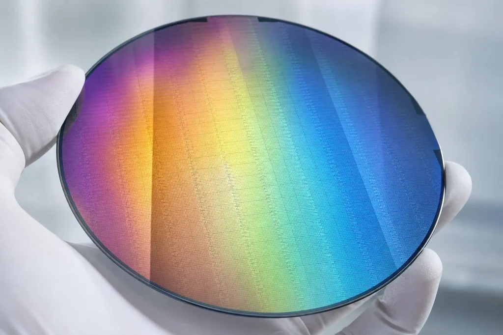
Semiconductor alloys are mixed crystals of two or more compound semiconductors, such as InxGa1−xN, AlxGa1−xAs and InGaAsP, whose bandgap and lattice constant can be set by composition. Bandgap engineering is the practice of choosing that composition to hit a target emission wavelength, barrier height or lattice match.
Key takeaways
- A ternary alloy mixes three elements (AlGaAs, InGaN); a quaternary mixes four (InGaAsP, AlGaInP). The quaternary adds a second degree of freedom, so bandgap and lattice constant can be tuned separately.
- Vegard’s law: the lattice constant varies linearly with composition. It holds to within a fraction of a percent for most III-V alloys.
- The bandgap does not vary linearly. It sags below the straight line by b·x(1−x), where b is the bowing parameter, in eV.
- Bowing is small in AlGaAs (near zero for the direct gap up to about x = 0.45) and large in InGaN (about 1.4 eV in widely used fits).
- InGaAsP lattice-matched to InP spans about 0.75 to 1.35 eV, which covers the 1.3 µm and 1.55 µm fibre bands.
What is a ternary semiconductor alloy?
A ternary alloy is a compound semiconductor with three elements on two sublattices. In a III-V crystal, group-III atoms (Al, Ga, In) sit on one sublattice and group-V atoms (N, P, As, Sb) on the other. AlxGa1−xAs is GaAs with a fraction x of the gallium sites taken by aluminium. The subscript x is the mole fraction, from 0 to 1. At x = 0 the crystal is pure GaAs; at x = 1 it is AlAs.
A quaternary alloy has four elements. It can mix on one sublattice (AlxGayIn1−x−yP) or on both (In1−xGaxAsyP1−y). The extra element matters because a ternary has one composition knob, so fixing the lattice constant also fixes the bandgap. A quaternary has two knobs. You can hold the lattice constant matched to a substrate and still move the bandgap across a useful range.
Alloys are random on their sublattice in the ideal case. Real alloys can cluster, order or phase-separate, and that changes their optical properties. For background on the binary compounds these alloys are built from, see the basics of compound semiconductors.
What is Vegard’s law?
Vegard’s law states that the lattice constant of an alloy is the composition-weighted average of its end points:
a(x) = x·aAC + (1−x)·aBC
For AlxGa1−xAs, aAC is the AlAs lattice constant (about 5.661 Å) and aBC is GaAs (5.653 Å at 300 K). The two differ by only about 0.15 %. That near-perfect match is why AlGaAs can be grown on GaAs at any composition without strain relaxation, and why it became the first workhorse heterostructure for lasers and HEMTs.
The nitrides are the opposite case. Wurtzite GaN has a = 3.189 Å; InN has a = 3.545 Å; AlN has a = 3.112 Å. InN and GaN differ by about 11 %. Vegard’s law still predicts the relaxed lattice constant of InxGa1−xN well, but a thin InGaN layer grown on GaN is compressively strained, and that strain feeds into polarization fields and defect formation.
Vegard’s law is an empirical rule. Small deviations exist, and for wide composition ranges some groups fit a small quadratic term. For epitaxy planning, the linear law is the standard starting point. The binary lattice constants for every material we cover are collected in the semiconductor materials index.
How does composition tune bandgap?
The bandgap is the energy gap between the top of the valence band and the bottom of the conduction band. It sets the photon energy a material emits or absorbs, through λ (nm) ≈ 1240 / Eg (eV). See energy bands and bandgap for the underlying band picture.
In an alloy, the bandgap moves between the two end-point values as composition changes. The standard expression is:
Eg(x) = x·Eg,AC + (1−x)·Eg,BC − b·x(1−x)
The first two terms are the linear interpolation. The third term is the bowing correction. It is zero at both end points and largest at x = 0.5, where it equals b/4.
Two complications appear in practice. First, the gap can switch from direct to indirect. In a direct gap the conduction band minimum and valence band maximum sit at the same crystal momentum, so light emission is efficient. In an indirect gap they do not. AlGaAs is direct up to about x = 0.45 and indirect above it, which is why AlGaAs light emitters stay below that composition. Second, strain shifts the gap. A layer pseudomorphically strained to a substrate has a slightly different gap from the same alloy fully relaxed.
What is bandgap bowing?
Bandgap bowing is the downward deviation of an alloy’s bandgap from linear interpolation. The bowing parameter b, in eV, measures its size. It arises because an alloy is not a perfect average crystal. Atoms of different size and electronegativity distort bond lengths and the local potential, which pulls the band edges together.
The cited example is InGaN. Using GaN at about 3.4 eV and InN at about 0.7 eV, with b ≈ 1.4 eV as in the fit of Wu and co-workers (Applied Physics Letters, 2002), the linear average at x = 0.3 would be about 2.6 eV. The bowing term subtracts about 0.3 eV, giving roughly 2.3 eV, which is green light near 540 nm. Ignoring bowing would put the same composition in the blue. Older work, before the InN gap was revised downward from about 1.9 eV, reported much larger and scattered bowing values. That history is why every InGaN number should be traced to its source.
For deeper detail on the InGaN case, including phase separation and the green gap, see our InGaN guide.
Common alloy systems compared
Values are approximate room-temperature figures from the recommended parameter sets of Vurgaftman, Meyer and Ram-Mohan (2001) and Vurgaftman and Meyer (2003, nitrides). Bowing parameters vary between studies, so ranges or typical fits are shown.
| Alloy | End points and bandgaps (eV, 300 K) | Bowing b (eV) | Usual substrate / match | Main uses |
|---|---|---|---|---|
| AlxGa1−xAs | GaAs 1.42 to AlAs 2.17 (indirect) | Near 0 for direct gap at low x | GaAs, matched at all x | Lasers, HEMT barriers, solar windows |
| InxGa1−xN | GaN about 3.4 to InN about 0.7 | About 1.4 (fits range higher) | GaN, strained; about 11 % end-point mismatch | Blue, green and white LEDs, laser diodes |
| AlxGa1−xN | GaN about 3.4 to AlN about 6.0 to 6.1 | About 0.7 to 1.0 | GaN or AlN, strained | HEMT barriers, UV LEDs |
| InxGa1−xAs | GaAs 1.42 to InAs 0.35 | About 0.5 | InP at x ≈ 0.53 (gap about 0.75) | Photodetectors, InP HEMTs |
| In1−xGaxAsyP1−y | About 0.75 to 1.35 when matched to InP | Composition dependent | InP | 1.3 µm and 1.55 µm telecom lasers |
| (AlxGa1−x)0.5In0.5P | About 1.9 to 2.3 (direct part) | Composition dependent | GaAs | Red and amber LEDs |
For side-by-side data on the binaries themselves, see the semiconductor comparison tables.
How is bandgap engineering used in devices?
Engineers use alloys for three jobs.
- Set the emission colour. The active region of a light emitter is an alloy whose gap matches the target wavelength. InGaN quantum wells give blue and green. AlGaInP gives red and amber. InGaAsP gives the near-infrared telecom bands.
- Build barriers and wells. A heterojunction is a junction between two different semiconductors. Placing a narrow-gap layer between wider-gap layers forms a quantum well that traps electrons and holes. The band offsets, set by alloy choice, decide how well carriers are confined. AlGaAs/GaAs and AlGaN/GaN are the classic pairs.
- Match or mismatch lattices on purpose. Lattice-matched alloys avoid misfit dislocations. Controlled mismatch adds strain, which shifts bands and, in the nitrides, adds piezoelectric polarization. Strained InGaAs channels in GaAs-based pHEMTs are a common example.
The telecom case shows why quaternaries matter. InP has a gap of about 1.35 eV. In0.53Ga0.47As, lattice-matched to InP, has about 0.75 eV. InGaAsP lets a designer choose any gap between those two while staying matched to InP. That is how laser and detector layers for 1.3 µm and 1.55 µm optical fibre are made. Our indium phosphide guide covers the InP platform in more depth.
Limits of bandgap engineering
- Miscibility gaps. Some alloys are thermodynamically unstable over part of their range and tend to separate into regions of different composition. InGaN at high indium content is the best-known case.
- Critical thickness. A strained layer can only grow so thick before misfit dislocations form to relieve the strain. The more mismatch, the thinner the limit.
- Direct-to-indirect crossover. Pushing AlGaAs or AlGaInP toward wider gaps eventually makes them indirect, and emission efficiency collapses.
- Doping gets harder in wide-gap alloys. Donor and acceptor levels deepen as aluminium content rises in AlGaN and AlGaAs, so fewer carriers are ionised at room temperature.
These limits explain why some colours and wavelengths are easy and others are not. Deep green, around 530 to 590 nm, sits beyond comfortable InGaN compositions and beyond the direct-gap range of AlGaInP, which is the root of the so-called green gap in LED efficiency.
Pick X when
- Pick AlGaAs for near-infrared and red emitters or barriers on GaAs, where lattice match at every composition makes growth simple.
- Pick InGaN for violet, blue and green emission on GaN, accepting strain and composition control challenges.
- Pick AlGaN for HEMT barriers and ultraviolet emitters, accepting harder doping at high aluminium content.
- Pick InGaAsP or InGaAs on InP for 1.3 µm to 1.55 µm lasers and detectors.
FAQ
Is the bandgap of an alloy always between its end points?
Usually, but not necessarily. With large bowing, the alloy gap near the middle of the range can fall below a simple average by several tenths of an eV. In extreme systems such as dilute nitrides (GaAsN), adding a small fraction of nitrogen lowers the gap below that of either end point.
Does Vegard’s law apply to bandgap?
No. Vegard’s law is for lattice constant. Applying linear interpolation to bandgap ignores bowing and can misplace an emission wavelength by tens of nanometres.
Why is AlGaAs so easy to grow on GaAs?
AlAs and GaAs have lattice constants within about 0.15 % of each other, so AlGaAs of any composition stays almost unstrained on a GaAs wafer.
What is the difference between ternary and quaternary alloys?
A ternary has three elements and one composition variable. A quaternary has four elements and two composition variables, so it can hold lattice match while the bandgap changes.
Sources
- I. Vurgaftman, J. R. Meyer and L. R. Ram-Mohan, “Band parameters for III-V compound semiconductors and their alloys,” Journal of Applied Physics (2001).
- I. Vurgaftman and J. R. Meyer, “Band parameters for nitrogen-containing semiconductors,” Journal of Applied Physics (2003).
- J. Wu et al., work on the InN bandgap and InGaN bowing, Applied Physics Letters (2002).
- S. M. Sze and K. K. Ng, Physics of Semiconductor Devices, 3rd ed., Wiley.
- Ioffe Institute, New Semiconductor Materials (NSM) archive, entries for GaAs, AlGaAs, GaN and InP.



