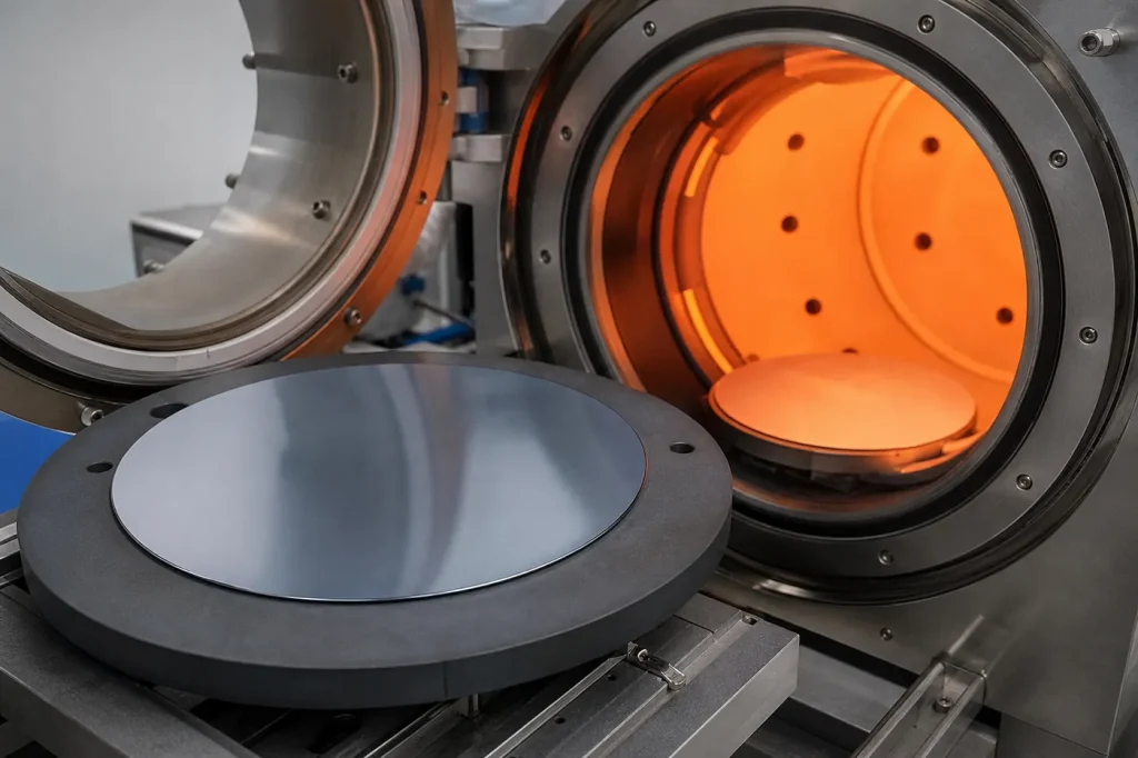
SiC epitaxy is grown by chemical vapour deposition (CVD) at about 1,500 to 1,650 °C from silane and a hydrocarbon such as propane, on 4H-SiC wafers cut 4° off the c-axis. The deciding factor is the off-cut. It creates atomic steps that let each new layer copy the 4H stacking, a mode called step-flow growth.
Key takeaways
- Standard substrate: 4H-SiC, Si-face, 4° off-axis toward the [11-20] direction. Older material used 8°.
- Standard chemistry: SiH4 plus C3H8 or C2H4 in hydrogen, often with chlorine added to allow faster growth.
- Growth temperature is about 1,500 to 1,650 °C in a hot-wall or warm-wall reactor at reduced pressure.
- Doping is set in situ: nitrogen for n-type, trimethylaluminium for p-type, both steered by the C/Si ratio.
- Most basal plane dislocations from the substrate convert to harmless threading edge dislocations at the epi interface. The few that survive cause bipolar degradation.
Why SiC devices need epitaxy at all
A SiC power MOSFET or Schottky diode blocks voltage in a lightly doped drift layer. That layer must have tightly controlled doping, often around 1015 to 1016 cm−3, and low defect density. Bulk SiC wafers from physical vapour transport cannot meet that spec. They are heavily doped, at roughly 1018 to 1019 cm−3 nitrogen, to act as a low-resistance substrate. So every SiC power device starts with an epitaxial drift layer grown on top. The wafer side of the story is in our guide to SiC wafers.
Drift-layer thickness scales with voltage rating. As a rule of thumb, a 1,200 V device uses on the order of 10 µm, and a 3.3 kV device on the order of 30 µm. Doping falls as the voltage rises. The exact numbers depend on the device design and the margin chosen.
Why are SiC wafers cut off-axis?
SiC exists in more than 200 polytypes, which are different stacking sequences of the same Si-C bilayers. 4H-SiC repeats every four bilayers. 3C-SiC, the cubic form, repeats every three and is stable at lower temperatures. On a perfectly flat (0001) surface, arriving atoms form new islands on the wide terraces. Those islands have no template for the stacking order and often nucleate as 3C-SiC. The result is a film full of 3C inclusions, which are fatal for devices.
Tilting the wafer a few degrees away from the c-axis creates a staircase of atomic steps. The terraces become narrow enough that adatoms (atoms diffusing on the surface) reach a step edge before they can nucleate an island. At the step edge, the exposed side of the crystal shows the 4H stacking, and the new atoms copy it. The film grows sideways from each step, which is why the mode is called step-flow growth. Kimoto, Matsunami and colleagues at Kyoto developed this “step-controlled epitaxy” approach.
The standard is 4° toward [11-20] for 4H-SiC on the Si-face. The industry moved down from 8° to save material, since a larger tilt wastes more of each boule when slicing, and to improve conversion of basal plane dislocations. A smaller off-cut has a cost. Wider terraces make step bunching more likely, where steps merge into rougher macro-steps, so growth conditions must be tighter. On-axis epitaxy is possible but needs careful process control.
How is SiC epitaxy grown? Step by step
- Prepare the substrate. The wafer arrives with a chemical-mechanical polished (CMP) Si-face. It is cleaned and loaded on a SiC-coated graphite susceptor.
- In-situ etch. The wafer is heated in hydrogen, sometimes with a little HCl or silane. This removes polishing damage and leaves a regular step structure.
- Grow the buffer layer. A thin, heavily doped n-type buffer, typically around 1018 cm−3, is grown first. It helps convert basal plane dislocations and, in many designs, speeds up recombination so holes injected from the device do not reach the substrate.
- Grow the drift layer. The hydrogen carrier gas carries the precursors over the wafer at about 1,500 to 1,650 °C and reduced pressure. Silane (SiH4) supplies silicon. Propane (C3H8) or ethylene (C2H4) supplies carbon. Nitrogen gas sets the n-type doping.
- Cool and inspect. Thickness is measured by FTIR (infrared reflectance) and doping by capacitance-voltage profiling, often with a mercury probe. Optical surface inspection maps particles and growth defects. UV photoluminescence imaging finds basal plane dislocations and stacking faults.
What temperature and chemistry does SiC epitaxy use?
| Parameter | Typical range or choice | Why it matters |
|---|---|---|
| Growth temperature | About 1,500 to 1,650 °C | High enough for long adatom diffusion and step flow |
| Silicon precursor | SiH4; or chlorinated sources such as SiHCl3 or SiCl4 | Chlorine suppresses silicon droplet formation in the gas phase |
| Carbon precursor | C3H8 or C2H4 | Sets the C/Si ratio with the silicon flow |
| Carrier gas | H2 | Transports precursors and etches the surface |
| C/Si ratio | Near 1, tuned by process | Controls dopant incorporation and morphology |
| n-type dopant | N2 | Nitrogen sits on carbon sites |
| p-type dopant | Trimethylaluminium (TMA) | Aluminium sits on silicon sites |
| Growth rate | A few to tens of µm/h in production; above 100 µm/h reported with chlorinated chemistry | Sets throughput for thick high-voltage layers |
| Reactor type | Hot-wall or warm-wall, horizontal or vertical; single or multi-wafer | Uniformity of thickness and doping |
The C/Si ratio is a key control knob because of a mechanism called site competition, described by Larkin and colleagues in the 1990s. Nitrogen competes with carbon for carbon sites, so a carbon-rich gas phase reduces nitrogen uptake. Aluminium competes with silicon for silicon sites, so carbon-rich conditions increase aluminium uptake. Growers use this to reach very low background doping in thick drift layers. For more on how dopants behave in SiC after growth, see our article on doping silicon carbide.
How are BPDs converted to TEDs?
SiC substrates contain two main classes of dislocation. Threading dislocations run roughly along the c-axis, through the wafer. Basal plane dislocations (BPDs) lie in the (0001) plane. Because the wafer is tilted 4°, a BPD in the substrate meets the surface at a shallow angle and can propagate into the epilayer.
Most do not. At the substrate-epi interface, a BPD tends to change direction and continue upward along the c-axis as a threading edge dislocation (TED). The driver is energy. A dislocation’s energy scales with its length. A line running nearly parallel to the surface through a 10 µm film is many times longer than one running straight up, so conversion to a TED lowers the total energy. The step-flow growth front also helps redirect the line. Kimoto and Cooper report conversion ratios well above 90% in standard processes, with optimised buffers and surface treatments pushing higher.
Why it matters: a BPD that survives into the drift layer can cause bipolar degradation. When the MOSFET’s body diode conducts, electrons and holes recombine at the BPD. The recombination energy drives the partial dislocations to glide, and the BPD expands into a Shockley stacking fault. Stacking faults act as barriers to current, so on-state voltage of the body diode rises over time. TEDs do not cause this effect.
Process levers that raise conversion or block the effect:
- Lower off-cut angles, which raise the energy penalty for a BPD to stay in the basal plane.
- In-situ etching or growth interruptions at the interface.
- A highly doped recombination-enhancing buffer, so holes recombine before reaching any BPD left near the substrate.
Other epitaxial defects to watch
- Carrot and triangular defects. Surface features nucleated by particles, substrate scratches or local polytype inclusions. They are classic device killers and are counted per wafer.
- Downfall. SiC deposits flaking off reactor walls onto the wafer. Reactor maintenance and design control it.
- Step bunching. Merged steps that roughen the surface and can degrade the gate oxide interface of a MOSFET.
- Point defects. The Z1/2 centre, linked to carbon vacancies, limits carrier lifetime. It matters most for bipolar devices such as PiN diodes and IGBTs.
For how the finished epiwafers turn into devices, see our silicon carbide hub and the overview of SiC power devices. Property data against other materials is in our comparison tables.
FAQ
Why is SiC epitaxy done on the Si-face?
The Si-face (0001) gives smoother step-flow growth, lower background doping and a better-understood gate oxide process. The C-face is used for some research devices but is less common in production.
Can SiC epitaxy be grown by MOCVD or MBE?
Not for power devices in practice. The high temperatures and thick layers favour hot-wall CVD with simple hydride or chloride precursors. MBE is used in research for thin layers.
What is the difference between a BPD and a TED?
Both are dislocations. A BPD lies in the basal (0001) plane and can expand into a stacking fault under bipolar current. A TED runs along the c-axis and is electrically benign in most devices.
Why add chlorine to the gas?
Silicon atoms in the gas phase tend to cluster into droplets at high silane flow. Chlorine binds silicon as chlorides and prevents this, which allows much higher growth rates without degrading the film.
Sources
- T. Kimoto and J. A. Cooper, Fundamentals of Silicon Carbide Technology, Wiley-IEEE Press, chapters on epitaxial growth and extended defects.
- T. Kimoto, A. Itoh and H. Matsunami, work on step-controlled epitaxy of SiC on off-axis substrates, Kyoto University.
- D. J. Larkin et al., “Site-competition epitaxy for superior silicon carbide electronics,” Applied Physics Letters (1994).
- H. Pedersen et al., “Chloride-based CVD growth of silicon carbide for electronic applications,” Chemical Reviews (2012).
- Ioffe Institute, New Semiconductor Materials (NSM) archive, SiC entry.