The SiC gate oxide is a thermally grown or deposited SiO2 layer that controls the channel of a SiC MOSFET. Its weak point is the interface. Defect densities there run tens to hundreds of times higher than on silicon, which cuts channel mobility to a few percent of bulk and makes the threshold voltage drift under bias and temperature.
Key takeaways
- Interface trap density near the conduction band is roughly 1012 to 1013 cm−2eV−1 as oxidised, against about 1010 for a good Si/SiO2 interface.
- Nitridation anneals in NO or N2O bring that down by about an order of magnitude and are standard in production.
- Channel mobility moves from single digits to roughly 20 to 50 cm²/V·s after nitridation, still far below about 1,000 cm²/V·s in bulk 4H-SiC.
- Threshold drift comes from charge trapping in the oxide near the interface. It is tested by bias-temperature stress, including gate-switching tests in JEDEC JEP184 and ECPE AQG 324.
- SiC’s higher permittivity pushes about 2.5 times more field into the oxide than into the semiconductor, which sets tight limits on gate design.
Why SiC can grow an oxide at all
SiC is the only wide-bandgap semiconductor that forms a native SiO2 layer by thermal oxidation, the same way silicon does. The carbon leaves as CO gas. This is a big part of why the SiC MOSFET reached volume production years ahead of other wide-gap MOSFETs. Oxidation is slower than on silicon, and the Si-face of 4H-SiC oxidises more slowly than the C-face. Many manufacturers now deposit the gate oxide and then anneal it, rather than growing all of it thermally.
The oxide itself is not the problem. The transition from SiC to SiO2 is. Our silicon carbide hub covers the wider device context.
What is interface trap density?
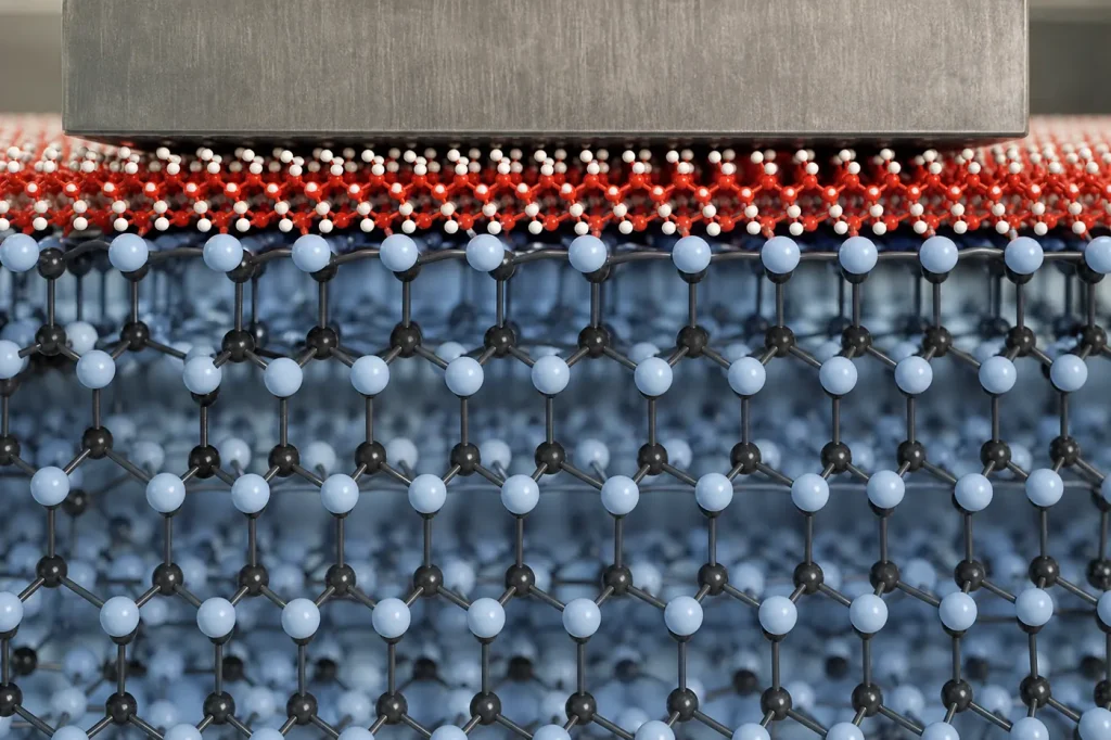
Interface trap density, written Dit, counts the electronic states at the semiconductor-oxide boundary that sit inside the bandgap. It is given per unit area per unit energy, in cm−2eV−1. Each trap can capture an electron from the channel. A captured electron no longer carries current, and its charge scatters the electrons that remain.
On SiC, these states cluster close to the conduction band edge, exactly where the inversion electrons of an n-channel MOSFET live. Proposed origins include carbon left behind at the interface, Si-O-C bonding defects and oxide defects lying a few nanometres into the SiO2, called near-interface traps. Afanas’ev and colleagues identified the near-interface oxide traps as a key contributor in work during the late 1990s.
| Interface / process | Dit near conduction band (cm−2eV−1) | Typical field-effect channel mobility (cm²/V·s) |
|---|---|---|
| Si / thermal SiO2 (reference) | About 1010 | Several hundred (electrons) |
| 4H-SiC (0001), dry oxidation, no anneal | About 1012 to 1013 | Below about 10 |
| 4H-SiC (0001), NO or N2O anneal | About 1011 to 1012 | About 20 to 50 |
| 4H-SiC (0001), phosphorus (POCl3) anneal, research | Lower than NO in reports | Up to roughly 80 to 90 reported |
| Bulk 4H-SiC electrons (no interface) | Not applicable | About 900 to 1,000 |
Why is SiC MOSFET channel mobility low?
Bulk electron mobility in 4H-SiC is close to silicon’s. The MOS channel loses most of it, for three reasons:
- Trapping. A large share of the electrons pulled to the interface by the gate fill traps instead of joining the channel. The free electron density is lower than the gate charge would suggest.
- Coulomb scattering. Filled traps are charged, and they scatter the free electrons travelling past them.
- Surface roughness and step bunching. Atomic-scale roughness at the interface scatters carriers at high gate fields.
The impact depends on voltage class. In a 1,200 V MOSFET, the drift layer contributes a large part of on-resistance, so channel resistance is one significant term among several. In a 650 V part, the drift layer is thinner and the channel is a bigger share of the total. That is part of why vendors work so hard on channel density and trench designs. Trench MOSFETs place the channel on a sidewall face, such as the a-face or m-face, where mobility can be higher than on the Si-face. Our SiC MOSFET vs Si IGBT comparison shows how this plays out in conduction loss.
What is an NO post-oxidation anneal?
A post-oxidation anneal (POA) is a heat treatment after the gate oxide forms. In the nitric-oxide version, the wafer is heated in NO gas, typically somewhere around 1,150 to 1,300 °C. Nitrogen diffuses through the oxide and collects at the SiC/SiO2 interface. There it passivates defect states, likely by removing carbon-related defects and bonding to dangling bonds. N2O anneals and oxidation in N2O work by a similar route.
Chung, Tin, Williams and colleagues reported in IEEE Electron Device Letters (2001) that high-temperature NO annealing substantially raised inversion channel mobility in 4H-SiC MOSFETs. Nitridation has been the production baseline since. It is effective but limited. Dit falls by about an order of magnitude, and mobility saturates in the tens of cm²/V·s.
Alternatives under study or in limited use:
- Phosphorus incorporation (POCl3 anneal). Higher mobility, but the phosphosilicate glass can make threshold voltage less stable.
- Deposited oxides with nitridation. Avoid consuming SiC and the carbon left behind by thermal oxidation.
- Interlayers and other dielectrics. Boron, alkaline-earth metals and high-k stacks have shown mobility gains in research. Reliability data at production scale is limited.
Why the oxide field is the design limit
Two physical facts squeeze the SiC gate oxide. First, by Gauss’s law the field in each material scales inversely with its permittivity. SiO2 has a relative permittivity of 3.9 and 4H-SiC about 9.7, so the oxide carries about 2.5 times the field of the SiC beneath it. Because SiC is designed to run at fields near 10 times silicon’s, the oxide at the trench corner or over the JFET region can see high stress in the off state.
Second, the conduction-band offset between SiO2 and 4H-SiC is smaller than on silicon, at roughly 2.7 eV in most reports against about 3.1 eV for SiO2/Si. A lower barrier allows more electron tunnelling into the oxide at high field and temperature. Designers use p-type shielding regions under trench bottoms and conservative oxide-field limits to protect the gate. Early-life oxide failures are screened with gate stress at the end of production.
What causes threshold voltage drift?
Threshold voltage (Vth) is the gate voltage at which the channel turns on. In SiC MOSFETs it shifts with bias and temperature, an effect called bias temperature instability (BTI). Lelis and colleagues at the US Army Research Laboratory showed that the main cause is electrons and holes tunnelling into and out of near-interface oxide traps.
- Positive BTI. Positive gate bias at high temperature traps electrons. Vth moves up and on-resistance rises.
- Negative BTI. Negative bias traps holes. Vth moves down, which can risk unwanted turn-on.
- Recovery. Part of the shift reverses within microseconds to seconds once stress is removed. The measured shift therefore depends on how fast the measurement follows the stress.
- Gate-switching instability. Repeated switching between negative off-bias and positive on-bias in an application can cause a cumulative drift that static DC tests do not capture.
How threshold stability is tested
- High-temperature gate bias (HTGB). Static positive and negative gate stress at maximum junction temperature, following JESD22 methods and AEC-Q101 for automotive discretes.
- JEDEC JEP184. A JC-70 guideline for evaluating BTI in SiC MOS devices. It addresses measurement timing and recovery so results can be compared.
- ECPE AQG 324. The European automotive qualification guideline for power modules. Recent versions add a dynamic gate stress test for SiC, applying fast bipolar gate switching to capture switching-induced drift.
- Time-dependent dielectric breakdown (TDDB). Accelerated gate-voltage stress to failure, used to extrapolate oxide lifetime at use conditions.
In practice, datasheets specify a recommended gate drive, commonly a positive on-voltage in the mid-to-high teens of volts and a turn-off voltage between 0 V and a few volts negative. Staying inside the supplier’s window is the simplest way to keep drift within the lifetime budget. Our overview of SiC power devices and the SiC material overview cover where these parts are used. Property data is in our comparison tables.
FAQ
Is SiC MOSFET gate oxide less reliable than silicon?
The intrinsic oxide can reach similar lifetimes at rated conditions. SiC has more extrinsic defects and higher field stress, so suppliers rely on screening and conservative gate ratings.
Why do SiC MOSFETs need a negative turn-off voltage?
Threshold voltage is relatively low and falls at high temperature. A negative off-bias gives margin against parasitic turn-on from fast voltage swings. Too much negative bias raises threshold drift, so suppliers specify a window.
Do GaN HEMTs have the same problem?
Not in the same form. Most GaN power HEMTs conduct through a polarisation-induced 2DEG with no MOS inversion channel. They have their own trapping issues, covered in GaN vs SiC.
What is the difference between Dit and near-interface traps?
Dit counts states at the boundary itself, which respond quickly. Near-interface traps sit a short distance inside the oxide and exchange charge by tunnelling, more slowly. Those slow traps drive most of the threshold drift.
Sources
- T. Kimoto and J. A. Cooper, Fundamentals of Silicon Carbide Technology, Wiley-IEEE Press, chapter on the SiC MOS interface.
- G. Y. Chung, C. C. Tin, J. R. Williams et al., “Improved inversion channel mobility for 4H-SiC MOSFETs following high temperature anneals in nitric oxide,” IEEE Electron Device Letters (2001).
- A. J. Lelis et al., work on bias temperature instability and threshold-voltage measurement in SiC MOSFETs, IEEE Transactions on Electron Devices.
- V. V. Afanas’ev et al., studies of intrinsic SiC/SiO2 interface states, physica status solidi (a).
- JEDEC JEP184 (BTI evaluation for SiC MOS devices); ECPE AQG 324 (automotive power module qualification); AEC-Q101.