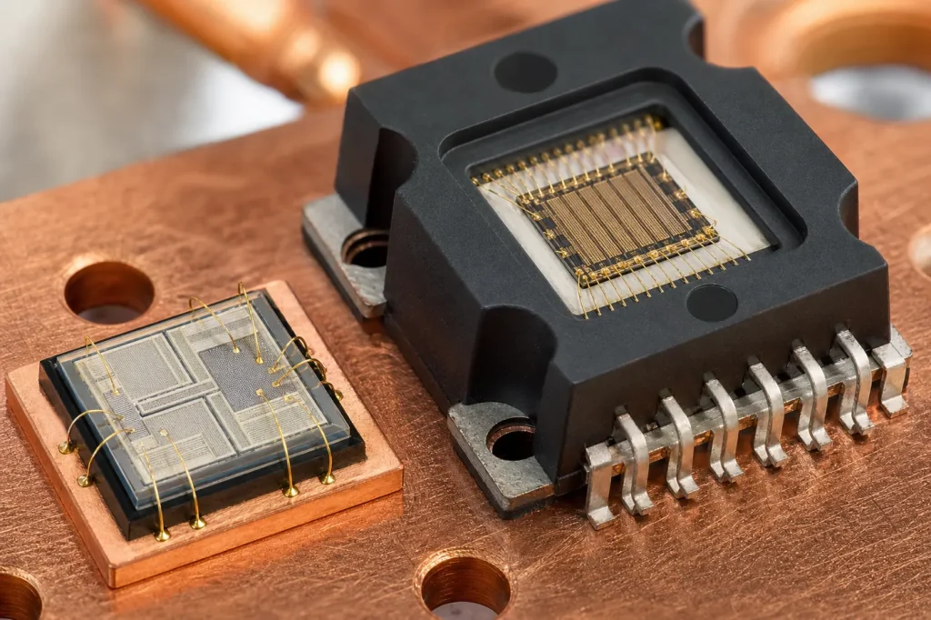
GaN vs SiC: GaN leads on switching speed, saturation velocity and channel mobility; SiC leads on thermal conductivity, avalanche ruggedness and voltage range. Both are wide-bandgap semiconductors near 3.3 eV. Pick GaN for compact, high-frequency converters at 650 V and below. Pick SiC for 1,200 V and above, including EV traction inverters.
Key takeaways
- Bandgap: GaN 3.39 eV vs 4H-SiC about 3.26 eV at 300 K. Critical field is similar, about 3.3 vs 2.5 to 3 MV/cm.
- GaN’s 2DEG mobility (about 1,500 to 2,000 cm²/V·s) is far above a SiC MOSFET channel, which is why GaN switches faster.
- SiC conducts heat about two to three times better (about 330 to 490 vs 130 to 230 W/m·K).
- Commercial GaN power parts cluster at 100 V to 650 V; SiC MOSFETs span 650 V to 1,700 V and up to 3.3 kV.
- The two meet head-on at 650 V, where the choice comes down to frequency, ruggedness and cost.
GaN vs SiC: material properties side by side
Values are for wurtzite GaN and 4H-SiC, the polytype used in power devices, at 300 K. Silicon is included as the baseline.
| Property (300 K) | GaN (wurtzite) | 4H-SiC | Si (reference) | Edge |
|---|---|---|---|---|
| Bandgap (eV) | 3.39, direct | 3.23 to 3.26, indirect | 1.12 | Roughly equal |
| Critical field (MV/cm) | About 3.3 (reported 3 to 5) | About 2.5 to 3 | About 0.3 | Slight GaN |
| Electron mobility, bulk (cm²/V·s) | Up to about 1,000 | About 900 to 1,000 | About 1,400 | Roughly equal |
| Electron mobility, device channel (cm²/V·s) | About 1,500 to 2,000 (AlGaN/GaN 2DEG) | Often well under 100 (MOS inversion channel) | Several hundred (MOS channel) | GaN |
| Saturation velocity (107 cm/s) | About 2.5 | About 2.0 | About 1.0 | GaN |
| Thermal conductivity (W/m·K) | About 130 to 230 | About 330 to 490 | About 130 to 150 | SiC |
| Static dielectric constant | About 8.9 | About 9.7 | 11.7 | Similar |
| Native substrate | Small and costly; usually grown on Si or SiC | 150 mm in volume, 200 mm ramping | 300 mm | SiC |
For the full GaN data set, including lattice constants and effective mass, see the GaN properties table. For more on SiC as a material, see our guide to silicon carbide in power electronics.
Which has the higher breakdown field, GaN or SiC?
On paper, GaN, slightly. The common design value for GaN is about 3.3 MV/cm. For 4H-SiC it is about 2.5 to 3 MV/cm, depending on doping. Both are roughly ten times silicon. The difference between them is small compared with the spread in published numbers, so treat them as comparable.
What matters more is how much of that field a real device can use. SiC devices are vertical: current flows from top to bottom through a thick, low-defect epitaxial drift layer on a conductive SiC wafer. The full material field is available, and voltage scales with drift-layer thickness. GaN power devices are mostly lateral HEMTs on silicon. Their voltage is limited by field crowding at the gate edge and by how much voltage the buffer can hold to the silicon below. That is why GaN’s slight material edge does not turn into higher voltage ratings. Our article on the breakdown field of semiconductors explains how critical field is measured and why values vary.
Why does GaN switch faster?
Three reasons, all rooted in device structure rather than bandgap.
- The 2DEG. A GaN HEMT conducts through a two-dimensional electron gas formed by polarisation at the AlGaN/GaN interface. Mobility is about 1,500 to 2,000 cm²/V·s at high sheet density. A SiC MOSFET conducts through an inversion channel under a gate oxide, where interface defects cut mobility to a small fraction of bulk. Higher channel mobility means a smaller die for the same on-resistance, and a smaller die has lower capacitance.
- Low gate and output charge. Lower capacitance means less charge to move each cycle. Switching edges are faster and the energy lost per transition is lower, which lets designers push frequencies into the hundreds of kHz or MHz range.
- No reverse recovery. A GaN HEMT has no p-n body diode. It conducts in reverse through the channel, with no stored minority charge to clear. SiC MOSFETs have a body diode with small but non-zero reverse recovery charge. In hard-switched bridge circuits such as totem-pole PFC, zero recovery is a real loss advantage.
The higher saturation velocity of GaN, about 2.5 × 107 cm/s against about 2.0 × 107 cm/s for SiC, matters most at RF, where it is one reason GaN dominates high-power microwave amplifiers.
Which has better thermal conductivity?
SiC, by a wide margin. 4H-SiC conducts about 330 to 490 W/m·K at 300 K. GaN sits at about 130 W/m·K for typical material and up to about 230 W/m·K for high-quality bulk crystals. In practice, GaN power devices are built on silicon (about 130 to 150 W/m·K), so the stack conducts heat no better than silicon.
This shapes applications. SiC handles high, sustained power and short-circuit events well because heat spreads quickly through the die. GaN relies on its lower losses to generate less heat in the first place, plus careful packaging. In RF, GaN is placed on SiC substrates precisely to borrow SiC’s thermal performance. See GaN-on-Si vs GaN-on-SiC for that substrate trade-off.
Typical commercial voltage classes
The table reflects the voltage ratings that appear across major suppliers’ catalogues as of 2025. It describes the general market, not any single product line. Check current datasheets before design work.
| Voltage class | GaN | SiC | Typical applications |
|---|---|---|---|
| Below 100 V to 200 V | Common (low-voltage e-mode HEMTs) | Not offered | 48 V DC-DC, lidar drivers, motor drives |
| 650 V / 700 V class | Common | Common (650 V and 750 V MOSFETs) | USB-C chargers, server and telecom PSUs, solar microinverters, onboard chargers |
| 1,200 V | Emerging, limited availability | Mainstream | 800 V EV traction inverters, industrial drives, solar string inverters |
| 1,700 V | Not commercial | Available | Auxiliary supplies, industrial converters |
| 3.3 kV and above | Not commercial | Available in limited volume | Rail traction, medium-voltage grid |
Which is better for EV inverters?
For the traction inverter, the unit that drives the motor, SiC is the established choice. Battery packs run at about 400 V or 800 V. An 800 V pack needs 1,200 V-rated switches, which is SiC’s core range. Traction inverters also handle hundreds of amps, need short-circuit withstand time and must survive load-dump and avalanche events. SiC MOSFETs are avalanche-rated and have the thermal headroom for this duty. Compared with silicon IGBTs, SiC lowers switching and conduction losses at partial load, which extends driving range. Our SiC MOSFET vs Si IGBT comparison covers that trade in detail.
GaN is moving into the onboard charger and DC-DC converter, where 650 V parts and high switching frequency shrink the magnetics. GaN in 400 V traction inverters is under active development, but SiC holds that market today.
Where do they overlap (650 V class)?
At 650 V both materials compete directly, and both beat silicon superjunction MOSFETs on switching loss. The choice depends on what the design optimises for.
- GaN wins on frequency and size. Laptop and phone chargers, high-density server power supplies and totem-pole PFC stages use GaN to run at higher frequency with smaller magnetics.
- SiC wins on ruggedness. SiC MOSFETs have avalanche capability and longer short-circuit withstand time. GaN HEMTs have no avalanche mechanism and are rated instead by transient overvoltage limits. Industrial and automotive designs that must survive fault events often prefer SiC.
- Gate drive differs. GaN e-mode HEMTs need a tight, low gate voltage window and careful layout. SiC MOSFETs use higher gate voltages and negative turn-off bias in many designs. Neither is a drop-in replacement for silicon.
Pick X when
- Pick GaN when the design is at 650 V or below and switching frequency, power density or efficiency at light load drive the decision: chargers, data-centre PSUs, 48 V conversion, class-D audio, lidar.
- Pick GaN when you need RF power at GHz frequencies. GaN-on-SiC is the standard for radar and base stations.
- Pick SiC when the bus voltage needs 1,200 V or higher switches: 800 V EV traction, solar string inverters, industrial drives, rail and grid.
- Pick SiC when thermal load, short-circuit withstand or avalanche ruggedness matter more than switching speed.
For the broader GaN device picture, see our overview of GaN for high-power applications.
FAQ
Is GaN or SiC more efficient?
It depends on the operating point. At 650 V and high switching frequency, GaN usually has lower switching loss. At 1,200 V and high current, SiC is usually more efficient and is the only one widely available.
Is GaN replacing SiC?
Not broadly. They overlap at 650 V, where GaN is taking share in consumer and data-centre power. Above about 900 V, SiC has no commercial GaN rival yet.
Why are SiC MOSFETs vertical and GaN HEMTs lateral?
SiC has large, conductive native wafers, so current can flow down through the substrate. GaN is usually grown on silicon, and its 2DEG forms at a surface interface, so current flows sideways near the top of the die.
Which has the wider bandgap, GaN or SiC?
GaN, slightly: 3.39 eV versus about 3.23 to 3.26 eV for 4H-SiC at 300 K. GaN’s gap is direct, which also makes it a light emitter; SiC’s is indirect.
Sources
- Ioffe Institute, New Semiconductor Materials (NSM) archive: http://www.ioffe.ru/SVA/NSM/Semicond/
- T. Kimoto and J. A. Cooper, Fundamentals of Silicon Carbide Technology, Wiley-IEEE Press.
- B. J. Baliga, Fundamentals of Power Semiconductor Devices, Springer.
- U. K. Mishra, P. Parikh and Y.-F. Wu, “AlGaN/GaN HEMTs: an overview of device operation and applications,” Proceedings of the IEEE (2002).
- S. M. Sze and K. K. Ng, Physics of Semiconductor Devices, 3rd ed., Wiley.



