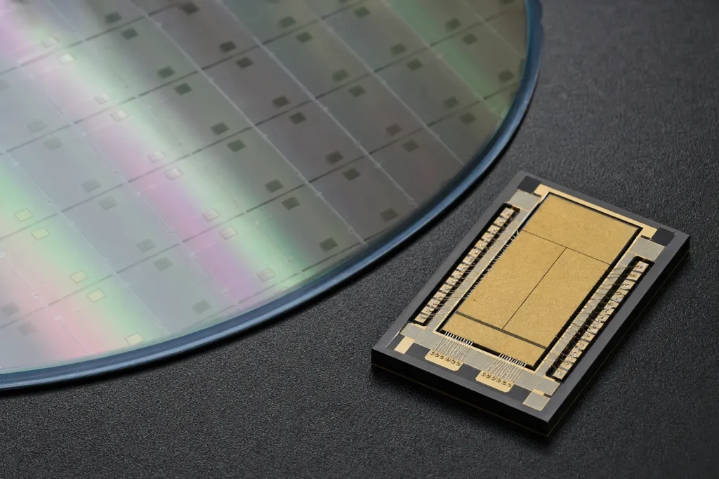
A wide-bandgap semiconductor is a semiconductor whose bandgap is well above silicon’s 1.12 eV, usually taken as about 2 to 3 eV or more. The wider gap lets it withstand a much higher electric field, run hotter and switch faster, which is why SiC and GaN now displace silicon in high-voltage power electronics.
Key takeaways
- There is no official cutoff. Most power-electronics literature treats gaps above roughly 2 to 3 eV as wide bandgap (WBG).
- The commercial WBG materials are 4H-SiC (about 3.26 eV) and GaN (3.39 eV), both at 300 K.
- Critical field rises steeply with bandgap: about 0.3 MV/cm for silicon versus about 3 MV/cm for SiC and GaN.
- A 10x higher critical field can cut the ideal drift-layer resistance by up to about 1,000x at the same voltage rating.
- Ultra-wide-bandgap (UWBG) materials such as Ga2O3, AlN and diamond have gaps above GaN’s 3.4 eV and remain mostly pre-commercial.
What counts as wide bandgap?
The bandgap is the energy an electron needs to jump from the valence band, where it is bound, to the conduction band, where it can carry current. Silicon’s gap is 1.12 eV at 300 K. GaAs sits at 1.42 eV. Both are considered conventional.
“Wide bandgap” is a working label, not a standard. Textbooks and reviews draw the line in slightly different places. Some use 2 eV, some about 2.3 eV, and power-device texts often just mean “SiC, GaN and anything wider.” What every definition agrees on is the comparison point: a WBG material has a gap at least two to three times silicon’s. For a wider tour of bandgap values, see our bandgap comparison across common semiconductors.
In practice, when an engineer says WBG today, they mean the two materials with real supply chains: silicon carbide (4H-SiC) and gallium nitride (GaN). Both crossed from research into volume production over the last two decades.
Which materials are wide bandgap?
The table compares silicon with the main WBG and UWBG candidates. Values are at 300 K. Critical field figures depend on doping and measurement method, so ranges are given where the literature disagrees.
| Material | Bandgap (eV, 300 K) | Critical field (MV/cm) | Electron mobility (cm²/V·s) | Thermal conductivity (W/m·K) | Status |
|---|---|---|---|---|---|
| Si | 1.12 (indirect) | About 0.3 | About 1,400 | About 130 to 150 | Mature baseline |
| 4H-SiC | 3.23 to 3.26 (indirect) | About 2.5 to 3 | About 900 to 1,000 (bulk) | About 330 to 490 | Volume production |
| GaN (wurtzite) | 3.39 (direct) | About 3.3 (reported 3 to 5) | Up to 1,000 bulk; about 1,500 to 2,000 in a 2DEG | About 130 to 230 | Volume production |
| β-Ga2O3 | About 4.6 to 4.9 | About 8 (estimated) | About 200 or less | About 10 to 27 (anisotropic) | Early commercial |
| Diamond | 5.47 (indirect) | About 10 or more (estimated) | About 2,000 (high-purity) | About 2,000 or more | Research |
| AlN (wurtzite) | 6.0 to 6.2 (direct) | About 12 or more (estimated) | About 300 | About 285 to 320 | Research for power; commercial in optics and RF filters |
Two details are easy to miss. First, SiC exists in many crystal stacking sequences called polytypes. 4H-SiC is the one used for power devices because it has higher electron mobility and less directional variation in mobility than the other common polytypes, such as 6H-SiC. Second, GaN’s headline mobility of about 2,000 cm²/V·s only applies to the two-dimensional electron gas (2DEG) at an AlGaN/GaN interface. Bulk GaN is lower. Our semiconductor properties table lists these materials alongside the conventional semiconductors.
Why does a wide bandgap allow higher voltage?
A semiconductor breaks down when the electric field inside it gets strong enough to trigger avalanche multiplication. A free electron accelerates, gains energy, and knocks a bound electron across the gap. That creates a new electron-hole pair, which repeats the process. Current then runs away.
The energy an electron must gain before it can ionise a bound electron scales with the bandgap. A wider gap means the carrier needs a stronger field to reach that energy between collisions. The result is a higher critical electric field, the field at which avalanche starts. Empirical fits across many materials put the critical field roughly proportional to the bandgap squared, so tripling the gap gives close to ten times the field. For the full set of measured and estimated values, see our guide to the breakdown field of semiconductors.
From critical field to lower resistance
The payoff shows up in the drift layer, the lightly doped region that holds off voltage in a power device. B. Jayant Baliga’s analysis gives the ideal specific on-resistance of that layer as:
Ron,sp = 4 BV² / (ε μ Ec³)
Here BV is the breakdown voltage, ε the permittivity, μ the electron mobility and Ec the critical field. The denominator, ε μ Ec³, is the Baliga figure of merit. Because Ec is cubed, a 10x higher critical field can lower the ideal resistance by up to about 1,000x for the same voltage rating, before the mobility difference is counted. In plain terms: a SiC or GaN die can block the same voltage as a silicon die while being much thinner and much smaller.
Smaller dies have lower capacitance. Lower capacitance means less energy lost each time the device switches. That is why WBG converters can run at higher switching frequencies, shrink their magnetics and capacitors, and still reach higher efficiency than silicon designs.
Higher temperature and lower leakage
A wider gap also suppresses thermally generated carriers. The intrinsic carrier concentration of 4H-SiC and GaN at 300 K is more than 15 orders of magnitude lower than silicon’s (about 1010 cm-3). Leakage stays low at temperatures where a silicon junction would stop blocking. In practice, packaging, gate oxides and contacts limit WBG operating temperature well before the semiconductor itself does.
SiC and GaN: the two commercial WBG materials
The two materials have similar gaps and critical fields but different strengths.
- SiC has two to three times the thermal conductivity of GaN and grows as large native wafers, so vertical MOSFETs and diodes are standard. It dominates from about 650 V up to 3.3 kV and beyond, including electric-vehicle traction inverters. See our overview of SiC wafers for diameters and defect issues.
- GaN is usually grown on silicon or SiC substrates as a lateral high-electron-mobility transistor (HEMT). Its 2DEG gives very low switching losses. It dominates fast-charging adapters and RF power amplifiers and competes with SiC at 650 V.
For the full side-by-side, including voltage classes and “pick X when” guidance, read GaN vs SiC.
What is ultra-wide bandgap?
Ultra-wide-bandgap (UWBG) semiconductors have gaps significantly larger than GaN’s 3.4 eV. The widely cited 2018 review by Tsao and co-authors uses that comparison as the working definition. The leading candidates are:
- β-Ga2O3 (gallium oxide), about 4.6 to 4.9 eV. It can be grown from the melt, which promises cheap large substrates. Its weaknesses are low thermal conductivity and no practical p-type doping.
- Diamond, 5.47 eV. It has the highest thermal conductivity of any bulk material and very high estimated critical field. Substrates are small and doping is hard.
- AlN and high-Al AlGaN, up to about 6.2 eV. Already used in deep-UV optoelectronics. Power devices are at the research stage.
- Cubic boron nitride, with a gap reported above 6 eV. It remains a laboratory material.
The common obstacle across UWBG materials is doping. As the gap widens, dopant energy levels sit deeper, so fewer of them release carriers at room temperature. Getting both n-type and p-type conduction in the same material is the main unsolved problem.
The trade-offs of going wide
A wider gap is not free. Wafers cost more per unit area than silicon and come in smaller diameters. Crystal defects such as basal plane dislocations in SiC and threading dislocations in GaN-on-Si affect yield and reliability. Gate oxides on SiC have lower channel mobility than the bulk, often well under 100 cm²/V·s. Many GaN HEMTs are normally-on by nature and need extra structures to turn off safely. These are the problems that occupy most WBG process engineers today.
FAQ
Is GaAs a wide-bandgap semiconductor?
No. GaAs has a gap of 1.424 eV at 300 K, close to silicon’s 1.12 eV. It is a compound semiconductor valued for electron mobility and light emission, not for high-voltage blocking.
Which wide-bandgap semiconductor has the highest thermal conductivity?
Diamond, at about 2,000 W/m·K or more. Among commercial WBG materials, 4H-SiC leads at roughly 330 to 490 W/m·K, about two to three times GaN.
Is a wider bandgap always better for power devices?
Not automatically. Critical field improves, but mobility, thermal conductivity, doping and substrate quality also decide performance. β-Ga2O3 has a wider gap than SiC but conducts heat more than ten times worse, which limits power density.
What does WBG stand for?
WBG stands for wide bandgap. UWBG stands for ultra-wide bandgap, the class beyond GaN’s 3.4 eV.
Sources
- Ioffe Institute, New Semiconductor Materials (NSM) archive: http://www.ioffe.ru/SVA/NSM/Semicond/
- B. J. Baliga, Fundamentals of Power Semiconductor Devices, Springer.
- T. Kimoto and J. A. Cooper, Fundamentals of Silicon Carbide Technology, Wiley-IEEE Press.
- J. Y. Tsao et al., “Ultrawide-Bandgap Semiconductors: Research Opportunities and Challenges,” Advanced Electronic Materials (2018).
- J. L. Hudgins et al., “An assessment of wide bandgap semiconductors for power devices,” IEEE Transactions on Power Electronics (2003).



