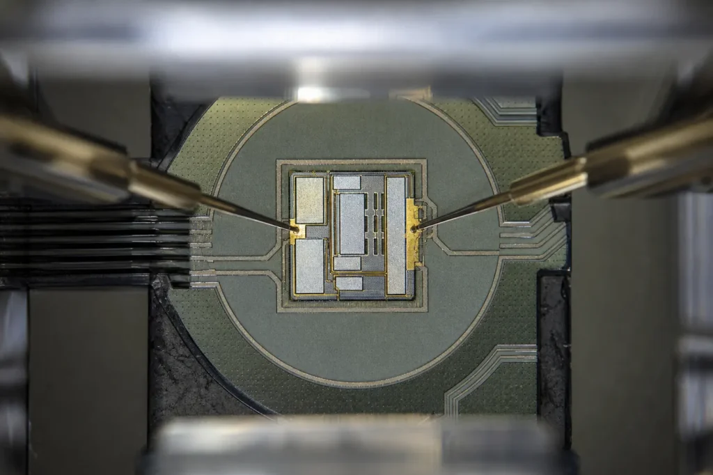
GaN reliability is the field of failure physics and qualification testing that decides whether a GaN transistor keeps its ratings over its service life. Its signature problem is charge trapping. Trapped electrons cause current collapse and dynamic on-resistance, effects silicon MOSFETs barely show, so GaN needs switching-mode tests on top of standard silicon qualification.
Key takeaways
- Current collapse is a temporary loss of drain current after high-voltage off-state stress. Electrons trapped at the surface or in the buffer deplete the 2DEG channel.
- Dynamic RDS(on) is the same effect seen in a power converter: on-resistance measured microseconds after turn-on is higher than the datasheet’s static value.
- The main fixes are SiN surface passivation, field plates that spread the gate-edge electric field, and carefully engineered carbon- or iron-doped buffers.
- JEDEC JEP173 covers dynamic on-resistance measurement. JEP180 covers switching reliability. Both add to, rather than replace, AEC-Q101 and JESD22 stress tests.
- GaN HEMTs have no avalanche mechanism, so overvoltage margin is specified differently from silicon and SiC.
What is current collapse in GaN?
Current collapse is a drop in the maximum drain current of a GaN high-electron-mobility transistor (HEMT) after the device has held a high drain voltage. The term comes from early RF work, where engineers saw output power at microwave frequencies fall well short of what DC curves predicted. Vetury and colleagues explained the main cause in IEEE Transactions on Electron Devices (2001): a “virtual gate”.
The mechanism is trapping. A trap is a defect state in the bandgap that can capture an electron and hold it for a time. Under high drain bias, the field at the drain-side edge of the gate is intense. Electrons leak from the gate onto the AlGaN surface, or are pushed into the GaN buffer below the channel, and get caught in traps. That trapped negative charge sits next to the channel and repels the electrons in the 2DEG, the two-dimensional electron gas that carries current. Part of the channel is pinched off by charge the gate no longer controls.
Traps release their electrons over time, so the effect recovers. Emission times range from microseconds to seconds or longer, depending on trap depth and temperature. That spread is why the result of a measurement depends so heavily on timing. Our article on defects in GaN covers the trap species in more detail.
What causes dynamic RDS(on)?
Dynamic RDS(on) is current collapse seen through a power-electronics lens. In a hard-switched converter, the transistor blocks the bus voltage while off, then turns on and must conduct full current within nanoseconds. If traps filled during the off state have not emptied, the channel is partly depleted and the on-resistance is higher than the static value. The ratio of dynamic to static RDS(on) is the usual figure of merit.
Four operating conditions make it worse:
- Higher off-state voltage. More field, more injected charge.
- Longer off-time. More time for slow traps to fill.
- Hard switching. Hot electrons generated during the overlap of voltage and current can be injected into traps. Soft-switched topologies are often gentler.
- Temperature. Heat speeds up trap emission, but it also raises static resistance and can activate different traps. The net effect is device-specific.
Higher conduction loss means more heat, which raises resistance again. In a well-designed part the effect is small and stable. In a poor one it can drive thermal runaway. Our GaN vs SiC comparison explains why GaN’s lateral structure makes surface and buffer physics so central.
Where traps live and how they are fixed
| Trap location | Origin | Symptom | Main mitigation |
|---|---|---|---|
| AlGaN surface | Dangling bonds and surface states between gate and drain | Virtual gate; collapse that recovers in ms to s | SiN passivation, often in situ; controlled surface clean |
| GaN buffer | Carbon or iron added to make the buffer insulating | Back-gating; slow recovery; voltage-dependent dynamic RDS(on) | Buffer doping profile, undoped channel spacer, leakage paths that let charge drain |
| Gate dielectric (MIS-HEMT) | Charge in or near the oxide or nitride interface | Threshold voltage shift | Dielectric choice and interface treatment |
| Gate edge, drain side | Peak electric field drives injection | Amplifies all of the above | Gate and source field plates; longer gate-drain spacing |
How field plates reduce collapse
A field plate is a metal electrode that extends from the gate, or from the source, over the passivation toward the drain. It reshapes the electric field. Without it, almost all of the drain voltage drops across a short region at the gate’s drain-side corner, and the field there peaks sharply. With one or more plates, the voltage drop is spread over a longer distance and the peak falls.
A lower peak field does three things. It reduces electron injection into surface and buffer traps, which cuts current collapse. It raises breakdown voltage. And it slows field-driven degradation at the gate edge. Field plates add capacitance, so RF designers use them sparingly. Power devices at 650 V often use several stacked plates. Some suppliers add a p-type GaN region near the drain that injects holes to neutralise trapped electrons. That approach is often called a hybrid-drain design.
Other GaN failure mechanisms
- Inverse piezoelectric effect. GaN is piezoelectric, so a high field strains the AlGaN barrier. Above a critical voltage, cracks and pits can form at the gate edge. Joh and del Alamo at MIT documented this in RF HEMTs. It is mainly a concern for depletion-mode RF parts under high reverse gate bias.
- Gate degradation in p-GaN e-mode devices. The p-GaN gate used in most normally-off power HEMTs tolerates only a few volts of overdrive. Excess gate voltage causes time-dependent breakdown, and threshold voltage can drift under bias.
- Hot-electron effects. High-energy electrons during hard switching create new traps over time, a slow wear-out path distinct from reversible trapping.
- Vertical leakage on silicon. In GaN-on-Si, the buffer must hold the full drain voltage to the substrate. Buffer leakage and breakdown set a voltage limit. See GaN-on-Si vs GaN-on-SiC.
- No avalanche. A silicon or SiC MOSFET can clamp an overvoltage spike by avalanching and absorbing the energy. A GaN HEMT has no p-n junction to avalanche. Suppliers instead rate transient overvoltage capability, and designers must keep spikes inside that limit.
How are GaN devices qualified?
GaN power parts are qualified in two layers. The first is the standard silicon stress suite. The second adds tests aimed at GaN-specific physics, guided by JEDEC committee JC-70, which handles wide-bandgap power semiconductors.
- Standard stress tests. These follow JESD22 methods and, for automotive discretes, AEC-Q101. They include high-temperature reverse bias (HTRB), high-temperature gate bias (HTGB), temperature cycling, high-humidity high-temperature reverse bias (H3TRB), intermittent operating life and ESD. They were written for silicon, so passing them is necessary but not sufficient.
- Dynamic on-resistance testing (JEP173). This guideline sets out how to measure dynamic RDS(on) in a switching circuit, including how to define timing, voltage and current so results are comparable between labs.
- Switching reliability (JEP180). This guideline describes how to stress devices under real hard-switching conditions over long periods, because DC stress alone misses hot-electron and dynamic trapping effects.
- Application-specific tests. Suppliers often add dynamic high-temperature operating life in a converter, short-circuit withstand and transient overvoltage tests. Test-to-fail data used to fit lifetime models is common.
Several GaN suppliers publish periodic reliability reports with stress results, acceleration models and field failure data. We do not quote their figures here because they are company claims that change with each edition. Ask for the latest report and check its test conditions against your application.
Is GaN as reliable as silicon?
Within its ratings, a qualified GaN power transistor is designed to meet the same lifetime and failure-rate targets as a silicon part in the same application. The differences lie in the failure modes and in the depth of field history.
- Different failure physics. Silicon MOSFET wear-out is dominated by gate oxide and well-understood hot-carrier effects. GaN adds trapping, buffer leakage and piezoelectric stress. Standard tests do not catch all of these, which is why JEP173 and JEP180 exist.
- Shorter field record. Silicon power MOSFETs have decades of fleet data. GaN power devices have had volume production for a much shorter time, mostly in consumer chargers, data centres and telecom supplies.
- Less forgiving gate and overvoltage limits. Silicon tolerates gate overshoot and avalanche events that a GaN HEMT does not. Layout, gate-drive design and snubbing matter more.
For where GaN power devices are used today, see the gallium nitride hub and our overview of GaN for high-power applications.
FAQ
Is current collapse permanent?
Usually not. Trapped charge empties over microseconds to seconds, faster when hot. Permanent change comes from new defects created by hot electrons or high fields, which is a separate wear-out process.
Why does a datasheet RDS(on) not match my converter?
Datasheet values are usually static, measured with low drain voltage before turn-on. In a converter the part has just blocked the bus voltage, so trapping raises the on-resistance. Check whether the supplier publishes dynamic values and under what conditions.
Is AEC-Q101 enough for automotive GaN?
It is the baseline, not the whole story. AEC-Q101 was written for silicon discretes. Automotive GaN programmes typically add switching-mode and dynamic on-resistance tests along the lines of JEP173 and JEP180.
Can GaN survive a short circuit?
For a limited time, set by the device and the gate drive. GaN dies are small and heat up fast, so short-circuit withstand time is generally shorter than for a SiC MOSFET. Fast desaturation protection is standard practice.
Sources
- R. Vetury, N. Q. Zhang, S. Keller and U. K. Mishra, “The impact of surface states on the DC and RF characteristics of AlGaN/GaN HFETs,” IEEE Transactions on Electron Devices (2001).
- M. Meneghini et al., “GaN-based power devices: physics, reliability and perspectives,” Journal of Applied Physics (2021).
- J. Joh and J. A. del Alamo, work on critical voltage and degradation of AlGaN/GaN HEMTs, IEEE Electron Device Letters and IEDM proceedings.
- JEDEC JC-70 guidelines JEP173 (dynamic on-resistance test methods for GaN power conversion devices) and JEP180 (switching reliability evaluation for GaN power conversion devices); JESD22 stress test methods.
- Automotive Electronics Council, AEC-Q101, stress test qualification for discrete semiconductors.



