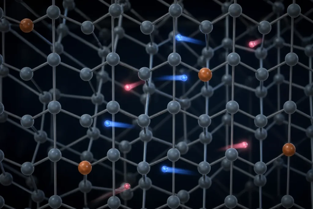
Doping is the deliberate addition of impurity atoms to a semiconductor to set its carrier type and concentration. Donors give up an electron and make the material n-type. Acceptors capture an electron, leaving a mobile hole, and make it p-type. Device doping usually runs from about 1014 to 1020 cm-3.
Key takeaways
- Intrinsic carrier density at 300 K is about 1010 cm-3 in Si and about 2 × 106 cm-3 in GaAs.
- In equilibrium n × p = ni2, so doping one carrier up pushes the other down.
- Shallow dopants in Si ionise fully at room temperature. Mg in GaN and Al in SiC are deep, so p-type doping is harder.
- Mobility falls as doping rises, because ionised impurities scatter carriers.
Common dopants by material
| Material | n-type (donors) | p-type (acceptors) | Approx. ionisation energy (eV) | Notes |
|---|---|---|---|---|
| Si | P, As, Sb | B | P 0.045, As 0.054, Sb 0.039; B 0.045 | All shallow; fully ionised at 300 K |
| GaAs | Si, Te, Se, S | Zn, Be, C | Donors about 0.006; acceptors about 0.03 | Si is amphoteric: it can sit on a Ga or an As site |
| 4H-SiC | N, P | Al, B | N about 0.05 to 0.1; Al about 0.2 | Dopants are implanted and annealed at high temperature |
| GaN | Si, Ge | Mg | Si about 0.015 to 0.03; Mg about 0.16 to 0.2 | Only a few percent of Mg acceptors ionise at 300 K |
What is doping?
A pure crystal is intrinsic. Its free electrons and holes come only from thermal excitation across the gap, and their density, ni, is small: about 1010 cm-3 in silicon at 300 K, against 5 × 10²² atoms per cm3. Doping makes the crystal extrinsic, with carriers supplied by impurities instead.
Doping levels are grouped loosely. Light doping, 1014 to 1016 cm-3, is used in drift and substrate regions. Heavy doping, above about 1019 cm-3 in Si, makes the material degenerate: the Fermi level enters a band and the semiconductor behaves almost like a metal. See Doping, Intrinsic Semiconductors and Extrinsic Semiconductors.
What are n-type and p-type semiconductors?
Silicon atoms have four valence electrons, each shared in a covalent bond. Phosphorus has five. Four bond, and the fifth is held so loosely (about 0.045 eV) that room-temperature heat frees it. The crystal becomes n-type, for negative carriers. Boron has three. The missing bond grabs an electron from a neighbour, and the vacancy moves through the lattice as a positive hole. The crystal becomes p-type.
Doped material stays electrically neutral: each free electron is balanced by a fixed, ionised donor. In compound semiconductors the same logic applies by site. Si on a Ga site in GaAs or GaN is a donor. Mg on a Ga site in GaN is an acceptor, but its depth and hydrogen passivation make p-GaN hard, covered in p-type GaN with magnesium. The FAQs What is n-type semiconductor? and What is p-type semiconductor? give short answers.
What are majority and minority carriers?
In equilibrium the product of electron and hole densities is fixed: n × p = ni2. This is the mass-action law. Dope silicon with 1016 donors per cm3 and n ≈ 1016 cm-3, so p ≈ 1020 / 1016 = 104 cm-3. Electrons are the majority carriers; holes are the minority carriers, twelve orders of magnitude fewer.
Majority carriers carry most of the current in resistors, MOSFET channels and Schottky diodes. Minority carriers govern p-n diodes, bipolar transistors and solar cells. Details are in Carrier Concentration and What do you mean by hole in semiconductor?.
What sets carrier mobility?
Mobility (μ, in cm²/V·s) is drift velocity per unit electric field. It equals qτ/m*, where τ is the mean time between collisions and m* is the effective mass. Two scattering mechanisms dominate: lattice vibrations (phonons), which worsen with temperature, and ionised dopants, which worsen with doping. Conductivity follows σ = q(nμn + pμp).
At 300 K and low doping, electron mobility is about 1,400 cm²/V·s in Si, about 8,500 in GaAs, up to about 1,000 in bulk GaN and about 900 in 4H-SiC. Hole mobility is lower in all of them: about 450 in Si and about 400 in GaAs. GaAs’s light electron mass explains its RF lead. See Mobility and the semiconductor properties table.
How do carriers recombine?
Excess electrons and holes, from light or injected current, recombine in three ways. Radiative recombination emits a photon and dominates in direct-gap GaAs and GaN. Shockley-Read-Hall recombination goes through defect levels in the gap and dominates in silicon. Auger recombination hands the energy to a third carrier and matters at high density.
The average time before recombination is the minority-carrier lifetime. It runs from nanoseconds in direct-gap material to microseconds or longer in high-purity silicon. Defects shorten it, which is why defect density in GaN matters for LED efficiency. The link to band structure is in the Energy Bands hub.
All doping and carrier guides
Core concepts
- Doping
- Intrinsic Semiconductors
- Extrinsic Semiconductors
- Carrier Concentration
- Mobility
- Conductivity
- Properties of Semiconductors
- Definition of Semiconductors
n-type, p-type and carriers
- What is n-type semiconductor?
- What is p-type semiconductor?
- What are p and n-type materials?
- Why is it called n-type?
- Why is it called p-type semiconductor?
- Why is n-type semiconductor neutral?
- How do you make a p-type semiconductor?
- What are the majority carriers in an n-type semiconductor?
- What do you mean by hole in semiconductor?
- What is the difference between an H type and a/p type intrinsic semiconductor?
Intrinsic vs extrinsic
- What is intrinsic and extrinsic semiconductor?
- What is difference between intrinsic and extrinsic semiconductor?
- What are intrinsic and extrinsic semiconductors give example?
- What is intrinsic semiconductor example?
- What is extrinsic semiconductor example?
- What are the two types of extrinsic semiconductor?
- Why do we need extrinsic semiconductors?
- How do you determine if a semiconductor is intrinsic or extrinsic?
- Is conductivity intrinsic or extrinsic?
- How can you increase the conductivity of an intrinsic semiconductor?
General semiconductor FAQs
- What are the main advantages of semiconductors over metals?
- Why are semiconductors special?
- Are semiconductors easily damaged by high temperature?
- What are the disadvantages of semiconductor?
- What are the advantages and disadvantages of semiconductor devices?
- What is the resistivity of a semiconductor?
- What is the principle of semiconductor?
- What are the 3 properties of semiconductors?
Related physics hubs
FAQ
Why is p-type GaN harder to make than n-type?
Magnesium, the only practical acceptor, sits about 0.16 to 0.2 eV above the valence band, so only a few percent ionise at room temperature. Hydrogen from growth also binds to Mg and must be driven out by annealing. Hole densities stay well below the Mg concentration.
Does doping change the bandgap?
Not at normal levels. Above roughly 1018 cm-3 in silicon, impurity bands merge with the band edge and the gap narrows by tens of meV, an effect called bandgap narrowing that matters in bipolar transistor emitters.
What doping does a typical silicon wafer have?
Standard CMOS substrates are lightly doped p-type, around 1015 cm-3 of boron, which gives a resistivity of order 10 Ω·cm. Transistor source and drain regions are doped far higher, above 1019 cm-3.
Sources
- S. M. Sze and K. K. Ng, Physics of Semiconductor Devices, 3rd ed., Wiley.
- C. Kittel, Introduction to Solid State Physics, 8th ed., Wiley.
- Ioffe Institute, New Semiconductor Materials (NSM) archive, http://www.ioffe.ru/SVA/NSM/Semicond/
